
- Catalogs
- Analog Devices
- SSM4567: Digital 2.5 W, 5.1 V, Boost Class-D Audio Amplifier with Output Sensing


- Products
- Catalogs
- News & Trends
- Exhibitions
SSM4567: Digital 2.5 W, 5.1 V, Boost Class-D Audio Amplifier with Output Sensing

SSM4567: Digital 2.5 W, 5.1 V, Boost Class-D Audio Amplifier with Output Sensing
- Filterless Class-D amplifier with spread-spectrum Σ-Δ modulation.
- Integrated boost regulator providing 5.1 V output.
- Supports PDM, TDM, and I2S data formats.
- Delivers 2.5 W into a 4 Ω load with less than 1% THD + N.
- High system efficiency of 89.7% into 8 Ω at 1 W.
- Advanced protection features including short-circuit and thermal protection.
- Output power: 2.5 W into 4 Ω, 1.42 W into 8 Ω at 3.6 V supply.
- THD + N: 0.025% at 1 kHz, 500 mW output power.
- Signal-to-noise ratio: 104 dB, A-weighted.
- Quiescent power consumption: 19.8 mW.
- Operating temperature range: -40°C to +85°C.
Catalog excerpts
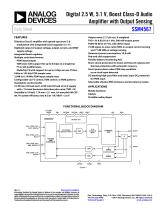
Digital 2.5 W, 5.1 V, Boost Class-D Audio Amplifier with Output Sensing SSM4567 Data Sheet FEATURES Output noise: 21.7 μV rms, A-weighted THD + N: 0.025% at 1 kHz, 500 mW output power PSSR: 90 dB at 217 Hz, with dither input 72 dB signal-to-noise ratio (SNR) on output current sensing and 77 dB SNR on voltage sensing Quiescent power consumption: 19.8 mW Pop-and-click suppression Flexible battery monitoring AGC Short-circuit protection for boost and Class-D outputs and thermal protection with automatic recovery Smart power-down when PDM stop condition or no clock input detected DC blocking high-pass filter and static input DC protection for PDM input Selectable ultralow EMI emissions and low latency modes Filterless Class-D amplifier with spread-spectrum Σ-Δ modulation with integrated boost regulator (5.1 V) Digitized output of output voltage, output current, and VBAT supply voltage Integrated boost regulator Multiple serial data formats PDM input/output TDM slave with support for up to 8 chips on a single bus I2S or left justified slave Multichip I2S with support for up to 4 chips on one I2S bus 8 kHz to 192 kHz PCM sample rates 2.048 to 6.14 MHz PDM input sample rates Configurable via I2C control, TDM control, or PDM patterns Standalone control modes 2.5 W into 4 Ω load and 1.42 W into 8 Ω load at 3.6 V supply with <1% total harmonic distortion plus noise (THD + N) Available in 19-ball, 1.74 mm × 2.1 mm, 0.4 mm pitch WLCSP 89.7% system efficiency into 8 Ω at 1 W, VBAT = 3.6 V APPLICATIONS Mobile handsets Tablets Portable media players FUNCTIONAL BLOCK DIAGRAM LR_SEL/ ADDR DAC_PDM_DAT/ DAC_SDATAI FILTERING MODULATION DAC_PDM_CLK/ BCLK SNS_PDM_CLK/ FSYNC SNS_PDM_DAT/ SNS_SDATAO Document Feedback Information furnished by Analog Devices is believed to be accurate and reliable. However, no responsibility is assumed by Analog Devices for its use, nor for any infringements of patents or other rights of third parties that may result from its use. Specifications subject to change without notice. No license is granted by implication or otherwise under any patent or patent rights of Analog Devices. Trademarks and registered trademarks are the property of their respective owners. One Technology Way, P.O. Box 9106, Norwood, MA 02062-9106, U.S.A. Tel: 781.329.4700 ©2014 Analog Devices, Inc. All rights reserved. Technical Support www.analog.com
Open the catalog to page 1
Data Sheet
Open the catalog to page 2
Data Sheet REVISION HISTORY 4/14—Revision 0: Initial Version
Open the catalog to page 3
Data Sheet GENERAL DESCRIPTION The SSM4567 is a digital input Class-D power amplifier that includes an integrated boost converter, allowing higher output power than with a normal battery supply. This means that maximum output power is constant across the battery voltage range. The SSM4567 is ideal for power sensitive applications where system noise can corrupt the small analog signal sent to the amplifier, such as mobile phones, tablets, and portable media players. The SSM4567 combines an audio digital-to-analog converter (DAC), a power amplifier, and PDM or PCM (I2S/TDM) digital audio interfaces...
Open the catalog to page 4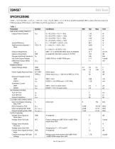
Data Sheet SPECIFICATIONS VBAT = 3.6 V, IOVDD = 1.8 V, TA = 25°C, RL = 8 Ω + 33 µH, VBST = 5.1 V, 20 Hz to 20 kHz bandwidth (BW), unless otherwise noted. In PDM operation, PDM clock = 3.072 MHz; for PCM operation, fS = 48 kHz. Table 1. Parameter AMPLIFIER CHARACTERISTICS Output Power/Channel System Efficiency Total Harmonic Distortion + Noise Output Voltage Noise Signal-to-Noise Ratio Average Switching Frequency Full-Scale Output Voltage Differential Output Offset Voltage POWER SUPPLIES Supply Voltage Range Power Supply Rejection Ratio Quiescent Supply Current VBAT IOVDD Shutdown Current VBAT...
Open the catalog to page 5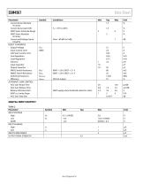
SSM4567 Parameter Current Sense Absolute Accuracy Current Sense Gain Drift VBAT Sense Full-Scale Range VBAT Sense Absolute Accuracy Current and Voltage Sense Linearity BOOST CONVERTER Output Voltage Input Current Limit Soft Start Current Limit Line Regulation Load Regulation Inductor Input Capacitor Output Capacitor PMOS Switch Resistance NMOS Switch Resistance Switching Frequency Efficiency AUTOMATIC GAIN CONTROL AGC Gain Attack Time AGC Gain Release Time Battery Inflection Point VBAT vs. Limiter Slope AGC Gain Step Size Data Sheet Symbol VOUT IMAX 1 10 10 RONP RONN fBOOSTSW ηBOOST VBAT = 3.6...
Open the catalog to page 6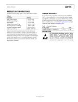
Data Sheet ABSOLUTE MAXIMUM RATINGS Absolute maximum ratings apply at 25°C, unless otherwise noted. VBAT Supply Voltage IOVDD Supply Voltage Storage Temperature Range Operating Temperature Range Junction Temperature Range Soldering Conditions Stresses at or above those listed under Absolute Maximum Ratings may cause permanent damage to the product. This is a stress rating only; functional operation of the product at these or any other conditions above those indicated in the operational section of this specification is not implied. Operation beyond the maximum operating conditions for extended...
Open the catalog to page 7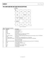
Data Sheet PIN CONFIGURATION AND FUNCTION DESCRIPTIONS BALL A1 INDICATOR 2 LR_SEL/ ADDR SNS_PDM_CLK/ FSYNC DAC_PDM_CLK/ BCLK SNS_PDM_DAT/ SNS_SDATAO Mnemonic IOVDD AGND PGND BSTSW LR_SEL/ADDR SEL SNS_PDM_CLK/FSYNC BSTSW DAC_PDM_CLK/BCLK SNS_PDM_DAT/SNS_SDATAO VBST VBST DAC_PDM_DAT/DAC_SDATAI PGND OUTN SCL OUTP VBAT SDA Description I/O and Digital Power Analog Ground Power Amplifier Ground Boost Switch Left or Right Selection for PDM Input/I2C Address PDM or I2S/TDM Interface Mode Select PDM Output Clock for Sense Data in PDM Mode/Frame Synchronization Clock in I2S/TDM Mode Boost Switch PDM Input...
Open the catalog to page 8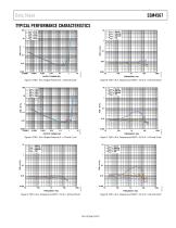
Data Sheet TYPICAL PERFORMANCE CHARACTERISTICS 100 POUT = 50mW POUT = 250mW POUT = 500mW POUT = 1W POUT = 50mW POUT = 250mW POUT = 500mW POUT = 1W Figure 6. THD + N vs. Frequency at VBAT = 4.2 V, RL = 8 Ω and 33 µH Figure 3. THD + N vs. Output Power at RL = 8 Ω and 33 µH POUT = 50mW POUT = 250mW POUT = 500mW POUT = 1W POUT = 50mW POUT = 250mW POUT = 500mW POUT = 1W Figure 7. THD + N vs. Frequency at VBAT = 3.6 V, RL = 8 Ω and 33 µH Figure 4. THD + N vs. Output Power at RL = 4 Ω and 15 µH 10 Figure 5. THD + N vs. Frequency at VBAT = 5 V, RL = 8 Ω and 33 µH Figure 8. THD + N vs. Frequency at VBAT...
Open the catalog to page 9All Analog Devices catalogs and technical brochures
 HMC722LP3E
8 Pages
 Isolated Sigma-Delta Modulator
17 Pages
 HMC853 Data Sheet
10 Pages
 AN-1084
8 Pages
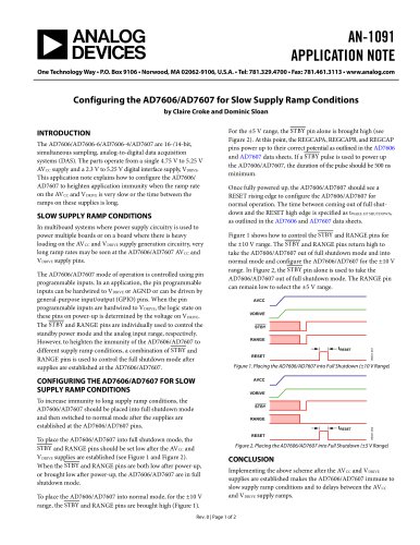 AN-1091
2 Pages
 AN_737
8 Pages
 AN-0982
4 Pages
 ADF7024
24 Pages
 AD9915
48 Pages
 AD9914
48 Pages
 ADRF6612
59 Pages
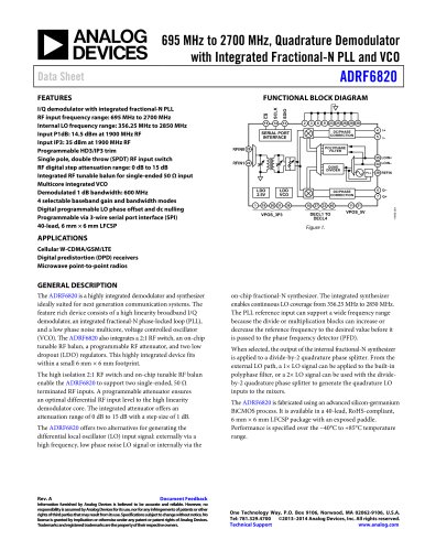 ADRF6820
48 Pages
 ADL5246
32 Pages
 ADA4961
22 Pages
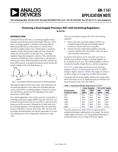 AN-1141
8 Pages
 AN-698
36 Pages
 Temperature Sensors
2 Pages
 Reference Circuits
8 Pages
 Precision ADCs
16 Pages
 ADR02ACHIPS: ADR02ACHIPS
8 Pages
 AD9364 RF Agile Transceiver
32 Pages
 Digital Temperature Sensors
2 Pages
 Digital to Analog Converter ICs
12 Pages
 AD1836A: Multichannel 96 kHz Codec
24 Pages




























Archived catalogs
 Zero-Drift Amplifiers
2 Pages
 Powering ADI Components
8 Pages




- Ethernet switch
- Industrial network switch
- Acceleration sensor
- Unmanaged switch
- Analog Devices motor controller
- Transceiver module
- Triaxial acceleration sensor
- DC motor controller
- Data acquisition unit
- Analog Devices stepper motor controller
- Industrial converter
- Ethernet transceiver
- Processor
- High-voltage amplifier
- Low-noise amplifier
- Multiplexer
- Compact motor controller
- Digital converter
- Closed-loop motor controller
- Digital motor controller