
- Catalogs
- Analog Devices
- Isolated Sigma-Delta Modulator


- Products
- Catalogs
- News & Trends
- Exhibitions
Isolated Sigma-Delta Modulator
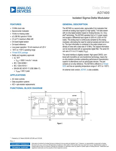
Isolated Sigma-Delta Modulator
- Operates at a 10 MHz clock rate with a second-order modulator.
- Provides 16-bit resolution with no missing codes and typical ±2 LSB INL at 16 bits.
- Maximum offset drift of 3.5 µV/°C and low power consumption at 18 mA maximum at 5.25 V.
- Functions within an operating temperature range from −40°C to +105°C.
- Includes on-board digital isolator and reference.
- Complies with safety and regulatory standards including UL 1577 and IEC/CSA.
- AC motor controls.
- Data acquisition systems.
- Replacement for A/D + opto-isolator.
The AD7400 is a sigma-delta modulator that converts an analog input signal to a high-speed, 1-bit data stream with on-chip digital isolation using iCoupler® technology. It operates from a 5 V power supply and accepts a differential input signal of ±200 mV. The device continuously samples the analog input, eliminating the need for external sample-and-hold circuitry. The serial interface is digitally isolated, providing superior performance compared to optocoupler devices.
- Resolution: 16 bits with filter output truncated to 16 bits.
- Integral Nonlinearity: ±15 LSB from −40°C to +85°C, ±25 LSB from >85°C to 105°C.
- Offset Error: ±0.5 mV with a drift of 3.5 µV/°C.
- Input Voltage Range: ±200 mV for specified performance, full range ±320 mV.
- Signal-to-Noise Ratio (SNR): 71 dB from −40°C to +105°C.
- Power Requirements: VDD1 = 4.5 V to 5.25 V, VDD2 = 3 V to 5.5 V.
- Rated Dielectric Insulation Voltage: 5000 V rms for 1 minute.
- Minimum External Air Gap (Clearance): 7.8 mm.
- Maximum Repetitive Isolation Voltage: 645 V peak.
The AD7400 has certifications from UL, CSA, and VDE, ensuring compliance with various safety standards for reinforced insulation and isolation voltages.
- VDD1 and VDD2: −0.3 V to +6.5 V.
- Operating Temperature Range: −40°C to +105°C.
- Storage Temperature Range: −65°C to +150°C.
The AD7400 is available in a 16-lead SOIC package with specific pin functions for supply voltage, analog inputs, and digital outputs.
Performance graphs illustrate PSRR, SINAD, offset drift, gain error drift, and other parameters across various conditions.
- Differential Nonlinearity: Difference between measured and ideal 1 LSB change between adjacent ADC codes.
- Integral Nonlinearity: Maximum deviation from a straight line through ADC transfer function endpoints.
- Offset Error: Deviation of midscale code from ideal input voltage.
- Gain Error: Deviation of full-scale codes from ideal values after offset error adjustment.
- SINAD: Ratio of signal to noise plus distortion, dependent on quantization levels.
- ENOB: Effective number of bits calculated from SINAD.
- THD: Ratio of rms sum of harmonics to the fundamental.
- CMRR: Ratio of power in ADC output to power of a sine wave applied to common-mode voltage.
- PSRR: Maximum change in full-scale transition point due to power supply voltage change.
- Isolation Transient Immunity: Rate of transient pulse beyond which data is corrupted.
The AD7400 is an isolated Σ-Δ modulator that converts an analog input into a high-speed single-bit data stream. The time average of this data is proportional to the input signal. The differential analog input uses a switched capacitor circuit to digitize the input signal into a 1-bit output stream. A Sinc3 filter is recommended for digital filtering and decimation to reconstruct the original signal.
The AD7400 uses a switched capacitor design for its differential inputs, requiring low common-mode noise for optimal performance. A recommended RC network helps manage charge spikes during sampling. A Sinc3 filter can be implemented on an FPGA or DSP for digital filtering.
Proper grounding and layout are crucial to minimize board coupling across the isolation barrier. Decoupling capacitors should be placed close to supply pins. Series resistance in analog inputs should be minimized to avoid distortion.
Evaluation boards are available for performance testing. The AD7400 is available in a 16-lead SOIC_W package, with options for different temperature ranges and compliance with RoHS standards.
Catalog excerpts
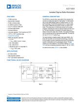
Data Sheet AD7400 Isolated Sigma-Delta Modulator FEATURES ► ► ► ► ► ► ► ► ► ► ► GENERAL DESCRIPTION 10 MHz clock rate Second-order modulator 16 bits no missing codes ±2 LSB INL typical at 16 bits 3.5 µV/°C maximum offset drift On-board digital isolator On-board reference Low power operation: 18 mA maximum at 5.25 V −40°C to +105°C operating range 16-lead SOIC package Safety and regulatory approvals ► UL 1577 ► VISO = 5000 V rms for 1 minute ► IEC / CSA 62368-1 ► IEC / CSA 61010-1 ► DIN EN IEC 60747-17 (VDE 0884-17) ► VIORM = 645 V peak The AD7400 is a second-order, sigma-delta (Σ-Δ) modulator that converts an analog input signal to a high speed, 1-bit data stream with on-chip digital isolation based on Analog Devices, Inc. iCoupler® technology. The AD7400 operates from a 5 V power supply and accepts a differential input signal of ±200 mV (±320 mV full scale). The analog input is continuously sampled by the analog modulator, eliminating the need for external sample-and-hold circuitry. The input information is contained in the output stream as a density of ones with a data rate of 10 MHz. The original information can be reconstructed with an appropriate digital filter. The serial I/O can use a 5 V or a 3 V supply (VDD2). The serial interface is digitally isolated. High speed CMOS, combined with monolithic air core transformer technology, means the on-chip isolation provides outstanding performance characteristics superior to alternatives such as optocoupler devices. The part contains an on-chip reference. The AD7400 is offered in a 16-lead SOIC and has an operating temperature range of −40°C to +105°C. An external clock version, AD7401, is also available. APPLICATIONS AC motor controls ► Data acquisition systems ► A/D + opto-isolator replacements FUNCTIONAL BLOCK DIAGRAM Rev. I DOCUMENT FEEDBACK TECHNICAL SUPPORT Information furnished by Analog Devices is believed to be accurate and reliable "as is". However, no responsibility is assumed by Analog Devices for its use, nor for any infringements of patents or other rights of third parties that may result from its use. Specifications subject to change without notice. No license is granted by implication or otherwise under any patent or patent rights of Analog Devices. Trademarks and registered tr
Open the catalog to page 1
Data Sheet
Open the catalog to page 2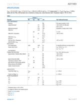
Data Sheet SPECIFICATIONS VDD1 = 4.5 V to 5.25 V, VDD2 = 3 V to 5.5 V, VIN+ = −200 mV to +200 mV, and VIN− = 0 V (single-ended); TA = TMIN to TMAX, fMCLK = 10 MHz, tested with Sinc3 filter, 256 decimation rate, as defined by Verilog code, unless otherwise noted. Temperature range is −40°C to +85°C. Table 1. Y Version1, 2 Parameter STATIC PERFORMANCE Resolution Integral Nonlinearity3 Differential Nonlinearity3 Offset Error3 ±50 Offset Drift vs. Temperature Offset Drift vs. VDD1 Gain Error3 Gain Error Drift vs. Temperature Gain Error Drift vs. VDD1 ANALOG INPUT Input Voltage Range Dynamic Input...
Open the catalog to page 3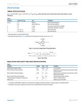
Data Sheet SPECIFICATIONS TIMING SPECIFICATIONS VDD1 = 4.5 V to 5.25 V, VDD2 = 3 V to 5.5 V, TA = TMAX to TMIN, unless otherwise noted. Sample tested during initial release to ensure compliance. Table 2. Parameter Limit at TMIN, TMAX Main clock output frequency Main clock output frequency Data access time after MCLK rising edge Data hold time after MCLK rising edge Main clock low time Main clock high time Mark space ratio for clock output is 40/60 to 60/40. Measured with the load circuit of Figure 2 and defined as the time required for the output to cross 0.8 V or 2.0 V. Figure 2. Load Circuit...
Open the catalog to page 4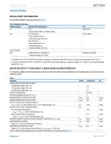
Data Sheet SPECIFICATIONS REGULATORY INFORMATION The AD7400 certification approvals are listed in Table 4. Table 4. Regulatory Information Regulatory Agency Standard Certification/Approval 1577 Single protection, 5000 V rms isolation voltage1 IEC / CSA 62368-1 Basic insulation, 780 V rms Reinforced insulation, 390 V rms IEC / CSA 61010-1 Basic Insulation, 600 V rms Overvoltage category III Reinforced insulation, 300 V rms In accordance with UL 1577, each AD7400 is proof tested by applying an insulation test voltage ≥ 6000 V rms for 1 second (current leakage detection limit = 15 µA). In accordance...
Open the catalog to page 5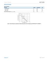
Data Sheet SPECIFICATIONS Table 5. (Continued) Description Case Temperature Side 1 Current Side 2 Current INSULATION RESISTANCE AT TS, VIO = 500 V Figure 4. Thermal Derating Curve, Dependence of Safety-Limiting Values with Case Temperature per DIN EN IEC 60747-17 (VDE 0884-17)
Open the catalog to page 6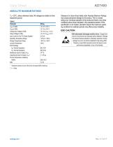
Data Sheet ABSOLUTE MAXIMUM RATINGS TA = 25°C, unless otherwise noted. All voltages are relative to their respective ground. Table 6. Parameter VDD1 to GND1 VDD2 to GND2 Analog Input Voltage to GND1 Output Voltage to GND2 Input Current to Any Pin Except Supplies1 Operating Temperature Range Storage Temperature Range Junction Temperature SOIC Package θJA Thermal Impedance θJC Thermal Impedance Resistance (Input-to-Output), RI-O Capacitance (Input-to-Output), CI-O2 Pb-Free Temperature, Soldering Reflow ESD ESD CAUTION ESD (electrostatic discharge) sensitive device. Charged devices and circuit boards...
Open the catalog to page 7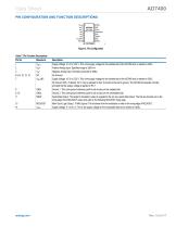
Data Sheet PIN CONFIGURATION AND FUNCTION DESCRIPTIONS Figure 5. Pin Configuration Table 7. Pin Function Descriptions Pin No. Supply Voltage. 4.5 V to 5.25 V. This is the supply voltage for the isolated side of the AD7400 and is relative to GND1. Positive Analog Input. Specified range of ±200 mV. Negative Analog Input. Normally connected to GND1. No Connect. Supply Voltage. 4.5 V to 5.25 V. This is the supply voltage for the isolated side of the AD7400 and is relative to GND1. No Connect (NC). If desired, Pin 7 may be allowed to float. It should not be tied to ground. The AD7400 will operate...
Open the catalog to page 8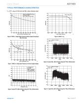
Data Sheet TYPICAL PERFORMANCE CHARACTERISTICS TA = 25°C, using a 20 kHz brick wall filter, unless otherwise noted. Figure 6. PSRR vs. Supply Ripple Frequency Without Supply Decoupling (1 MHz Filter Used) Figure 7. SINAD vs. Analog Input Frequency for Various Supply Voltages Figure 10. Typical DNL, ±200 mV Range (Using Sinc3 Filter, 256 Decimation Rate) Figure 8. Typical FFT, ±200 mV Range (Using Sinc3 Filter, 256 Decimation Rate) Figure 11. Typical INL, ±200 mV Range (Using Sinc3 Filter, 256 Decimation Rate)
Open the catalog to page 9All Analog Devices catalogs and technical brochures
 HMC722LP3E
8 Pages
 HMC853 Data Sheet
10 Pages
 AN-1084
8 Pages
 AN-1091
2 Pages
 AN_737
8 Pages
 AN-0982
4 Pages
 ADF7024
24 Pages
 AD9915
48 Pages
 AD9914
48 Pages
 ADRF6612
59 Pages
 ADRF6820
48 Pages
 ADL5246
32 Pages
 ADA4961
22 Pages
 AN-1141
8 Pages
 AN-698
36 Pages
 Temperature Sensors
2 Pages
 Reference Circuits
8 Pages
 Precision ADCs
16 Pages
 ADR02ACHIPS: ADR02ACHIPS
8 Pages
 AD9364 RF Agile Transceiver
32 Pages
 Digital Temperature Sensors
2 Pages
 Digital to Analog Converter ICs
12 Pages
 AD1836A: Multichannel 96 kHz Codec
24 Pages




























Archived catalogs
 Zero-Drift Amplifiers
2 Pages
 Powering ADI Components
8 Pages




- Ethernet switch
- Industrial network switch
- Acceleration sensor
- Unmanaged switch
- Analog Devices motor controller
- Transceiver module
- Triaxial acceleration sensor
- DC motor controller
- Analog Devices stepper motor controller
- Industrial converter
- Ethernet transceiver
- Processor
- High-voltage amplifier
- Low-noise amplifier
- Multiplexer
- Compact motor controller
- Digital converter
- Closed-loop motor controller
- Digital motor controller