- Catalogs
- Analog Devices
- HMC722LP3E
HMC722LP3E
1 /8Pages

HMC722LP3E
1 /8Pages
Catalog excerpts

13 Gbps, FAST RISE TIME AND/NAND/OR/NOR GATE, w/ PROGRAMMABLE OUTPUT VOLTAGE HIGH SPEED LOGIC - SMT Typical Applications Supports High Data Rates: up to 13 Gbps Differential & Singe-Ended Operation • Broadband Test & Measurement Fast Rise and Fall Times: 19 / 18 ps • Serial Data Transmission up to 13 Gbps • Digital Logic Systems up to 13 GHz Programmable Differential Output Voltage Swing: 600 - 1100 mV • NRZ-to-RZ Conversion Propagation Delay: 95 ps Single Supply: -3.3V 16 Lead 3x3 mm SMT Package: 9 mm² Functional Diagram General Description The HMC722LP3E is an AND/NAND/OR/NOR function designed to support data transmission rates of up to 13 Gbps, and clock frequencies as high as 13 GHz. The HMC772LP3E may be easily configured to provide any of the following logic functions: AND, NAND, OR and NOR. The HMC722LP3E also features an output level control pin, VR, which allows for loss compensation or for signal level optimization. All input signals to the HMC722LP3E are terminated with 50 Ohms to ground on-chip, and may be either AC or DC coupled. The differential outputs of the HMC722LP3E may be either AC or DC coupled. Outputs can be connected directly to a 50 Ohm to ground terminated system, while DC blocking capacitors may be used if the terminating system is 50 Ohms to a non-ground DC voltage. The HMC722LP3E operates from a single -3.3V DC supply, and is available in a RoHS compliant 3x3 mm SMT package. Electrical Specifications, TA = +25 °C, Vee = -3.3V Parameter Power Supply Voltage Power Supply Current Maximum Data Rate Maximum Clock Rate Input High Voltage Input Return Loss Output Amplitude Output High Voltage Single-Ended, peak-to-peak Differential, peak-to-peak Information furnished by Analog Devices is believed to be accurate and reliable. However, no For price, 20 delivery, and to place orders: Analog For price, delivery and to place orders: Microwave Corporation, Alpha Road, Chelmsford, MADevices, 01824 Inc., responsibility is assumed by Analog Devices for its use, nor for anyHittite infringements of patents or other One Technology Way, P.O. Box 9106, Norwood, MA 02062-9106 rights of third parties that may result from its use. Specifications subject to change without notice. No Phone: 978-250-3343 Fax: 978-250-3373 Order at www.hittite.com Phone: On-line 781-329-4700 • Order online at www.analog.com license is granted by implication or otherwise under any patent or patent rights of Analog Devices. Application Support: Phone: 1-800-ANALOG-D Trademarks and registered trademarks are the property of their respective owners. Application Support: Phone: 978-250-3343 or apps@
Open the catalog to page 1
13 Gbps, FAST RISE TIME AND/NAND/OR/NOR GATE, w/ PROGRAMMABLE OUTPUT VOLTAGE Electrical Specifications, (continued) Conditions Output Rise / Fall Time Output Return Loss Small Signal Gain Random Jitter Jr peak-to-peak, 215 -1 PRBS input [1] Deterministic Jitter, Jd Propagation Delay, td [1] Deterministic jitter calculated by simultaneously measuring the jitter of a 300 mV, 13 GHz, 215 -1 PRBS input, and a single-ended output DC Current vs. Supply Voltage Output Differential vs. Supply Voltage [1] [3] Output Differential vs. Frequency [3] 1300 Output Differential vs. VR [2] DIFFERENTIAL VOLTAGE...
Open the catalog to page 2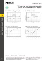
13 Gbps, FAST RISE TIME AND/NAND/OR/NOR GATE, w/ PROGRAMMABLE OUTPUT VOLTAGE Rise / Fall Time vs. Supply Voltage [3] Rise / Fall Time vs. VR [3] Input Return Loss vs. Frequency Output Return Loss vs. Frequency -10 HIGH SPEED LOGIC - SMT Information furnished by Analog Devices is believed to be accurate and reliable. However, no For price, 20 delivery, and to place orders: Analog For price, delivery and to place orders: Microwave Corporation, Alpha Road, Chelmsford, MADevices, 01824 Inc., responsibility is assumed by Analog Devices for its use, nor for anyHittite infringements of patents or other...
Open the catalog to page 3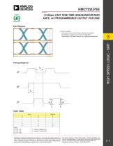
13 Gbps, FAST RISE TIME AND/NAND/OR/NOR GATE, w/ PROGRAMMABLE OUTPUT VOLTAGE Eye Diagram 3 HIGH SPEED LOGIC - SMT [1] Test Conditions: Pattern generated with an Agilent N4903A Serial BERT. Eye Diagram presented on a Tektronix CSA 8000. Device input = 10 Gbps PN code, Vin = 300mVp-p differential. Timing Diagram Truth Table Input H - Positive voltage level L - Negative voltage level Information furnished by Analog Devices is believed to be accurate and reliable. However, no For price, 20 delivery, and to place orders: Analog For price, delivery and to place orders: Microwave Corporation, Alpha...
Open the catalog to page 4
13 Gbps, FAST RISE TIME AND/NAND/OR/NOR GATE, w/ PROGRAMMABLE OUTPUT VOLTAGE Absolute Maximum Ratings HIGH SPEED LOGIC - SMT Power Supply Voltage (Vee) Input Signals Output Signals Storage Temperature Operating Temperature ELECTROSTATIC SENSITIVE DEVICE OBSERVE HANDLING PRECAUTIONS Outline Drawing NOTES: 1. LEADFRAME MATERIAL: COPPER ALLOY 2. DIMENSIONS ARE IN INCHES [MILLIMETERS] 3. LEAD SPACING TOLERANCE IS NON-CUMULATIVE 4. PAD BURR LENGTH SHALL BE 0.15mm MAXIMUM. PAD BURR HEIGHT SHALL BE 0.05mm MAXIMUM. 5. PACKAGE WARP SHALL NOT EXCEED 0.05mm. 6. ALL GROUND LEADS AND GROUND PADDLE MUST BE...
Open the catalog to page 5
13 Gbps, FAST RISE TIME AND/NAND/OR/NOR GATE, w/ PROGRAMMABLE OUTPUT VOLTAGE Pin Descriptions Function Signal Grounds Clock / Data Input A Clock / Data Input B Clock / Data Output Supply Ground Output level control. Output level may be adjusted by either applying a voltage to VR per “Output Differential vs. VR” plot. Negative Supply Interface Schematic Information furnished by Analog Devices is believed to be accurate and reliable. However, no For price, 20 delivery, and to place orders: Analog For price, delivery and to place orders: Microwave Corporation, Alpha Road, Chelmsford, MADevices,...
Open the catalog to page 6
13 Gbps, FAST RISE TIME AND/NAND/OR/NOR GATE, w/ PROGRAMMABLE OUTPUT VOLTAGE Evaluation PCB HIGH SPEED LOGIC - SMT List of Materials for Evaluation PCB 118777 [1] Item HMC722LP3E High Speed Logic, AND / NAND / OR / NOR [1] Reference this number when ordering complete evaluation PCB [2] Circuit Board Material: Rogers 4350 or Arlon 25FR The circuit board used in the application should use RF circuit design techniques. Signal lines should have 50 Ohm impedance while the package ground leads should be connected directly to the ground plane similar to that shown. The exposed package base should be...
Open the catalog to page 7All Analog Devices catalogs and technical brochures
 Isolated Sigma-Delta Modulator
17 Pages
 HMC853 Data Sheet
10 Pages
 AN-1084
8 Pages
 AN-1091
2 Pages
 AN_737
8 Pages
 AN-0982
4 Pages
 ADF7024
24 Pages
 AD9915
48 Pages
 AD9914
48 Pages
 ADRF6612
59 Pages
 ADRF6820
48 Pages
 ADL5246
32 Pages
 ADA4961
22 Pages
 AN-1141
8 Pages
 AN-698
36 Pages
 Temperature Sensors
2 Pages
 Reference Circuits
8 Pages
 Precision ADCs
16 Pages
 ADR02ACHIPS: ADR02ACHIPS
8 Pages
 AD9364 RF Agile Transceiver
32 Pages
 Digital Temperature Sensors
2 Pages
 Digital to Analog Converter ICs
12 Pages
 AD1836A: Multichannel 96 kHz Codec
24 Pages


Archived catalogs
 Zero-Drift Amplifiers
2 Pages
 Powering ADI Components
8 Pages


- Ethernet switch
- Industrial network switch
- Acceleration sensor
- Unmanaged switch
- Transceiver module
- Analog Devices motor controller
- Triaxial acceleration sensor
- DC motor controller
- Data acquisition unit
- Analog Devices stepper motor controller
- Industrial converter
- Ethernet transceiver
- Processor
- High-voltage amplifier
- Low-noise amplifier
- Multiplexer
- Compact motor controller
- Gyroscope
- Closed-loop motor controller
- Digital converter