- Catalogs
- Analog Devices
- AN-1141
AN-1141
1 /8Pages

AN-1141
1 /8Pages
Catalog excerpts

AN-1141 APPLICATION NOTE One Technology Way • P.O. Box 9106 • Norwood, MA 02062-9106, U.S.A. • Tel: 781.329.4700 • Fax: 781.461.3113 • www.analog.com Powering a Dual Supply Precision ADC with Switching Regulators by Rui Du INTRODUCTION Compared with an LDO device, a switching regulator always dissipates much less heat and provides higher efficiency. Therefore, a switching regulator is suitable for powering different kinds of portable devices or the nodes in a wireless sensor network to lengthen battery time. Unfortunately, a switching regulator intrinsically generates ripple and noise at both the output rail and the ground. At the same time, a switching regulator brings electromagnetic radiation. These interferences are almost inevitable due to the continuously on-off operation of the power switch. With the parasitic parameters involved, the noise will be present at unexpected frequency points besides the integer multiple of the switching frequency. Figure 1. Typical Ripple and Noise at the Output of a Switching Regulator Although damaged from the noise issues, if the interference of the switching regulator can be effectively controlled while the circuit is powered by a switching regulator, which has a strong anti-interference capacity, then the degrading of the system performance will be slight. For a typical application, when a data converter is powered by a switching mode power supply (SMPS), keep the total noise over the band of interest lower than the noise floor to prevent it from being seen by the converter. Although the in-band noise from the switching regulator is normally greater than the noise floor, because of the power rejection ratio of the ADC, the noise will be sharply attenuated before entering the signal path; as a result, the switching noise will not degrade the performance of the ADC. There are two options to power the ADC with switching regulators: A. Select a low noise switching regulator and then use carefully designed filtering and shielding methods to remove as much of the noise as possible. B. Estimate the noise suppressing capability of the data converter, and then select the product, which has good noise-immunity performance. In practice, both options can be used at the same time so that the power solution of using a switching regulator can be acceptable in most cases. The switching regulator solution includes the benefits of high efficiency and low temperature. In CN-0137, a dual-output synchronous buck switching regulator, ADP2114, is used to power the 16-bit, 125 MSPS analog-to-digital converter, AD9268. The outputs of ADP2114 are filters using an extra stage of an LC filter (ferrite bead). Compared with the linear supplies solution, the testing result shows that using a dc-to-dc supply has nearly no influences on the performance of the ADC (see Table 1). Table 1. Experiment Results Reported in CN-0137 Analog Input Frequency (MHz) 10.3 70.0 100.3 140.3 170.3 200.3 The noise performance of the ADP2114 is guaranteed by multiple technologies implemented in the design. The typical voltage ripple is less than 1 mV. Using additional filtering, its noise performance can even align with linear supplies.
Open the catalog to page 1
REVISION HISTORY
Open the catalog to page 2
Application Note In this application note, a switching regulator is used to power the ADC without any additional filtering or shielding measures, only the necessary external components kept for normal operation of the dc-to-dc power supply. According to the second option mentioned previously, two power-insensitive ADCs, the AD7610 and AD7612 are used for testing. This application note aims at finding out how much harm is brought by the SMPS to the ADC and whether it is acceptable. Figure 4. Analog Input CMRR vs. Frequency of AD7610 or AD7612 More importantly, the AD7610 and AD7612 provide excellent...
Open the catalog to page 3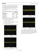
Application Note For a SMPS, the output-voltage ripple can be suppressed by using a big inductor and output capacitor in the topology. To deal with the switching noise, an extra filter at the output can be used. By doing this, the PCB area will be sacrificed. The basic configuration of the 5 V to ±12 V power modules is shown in Table 2. Configuration Switching Frequency Output Inductor Input Capacitor Output Capacitor Maximum Load Figure 8. AC-Coupled Output Voltage of the −12 V Rail T Note the following about the ripple and noise performance under the typical loading (50% of full load): • Table...
Open the catalog to page 4
Application Note The first experiment was performed based on AD7612-EVAL and ADuC7026-EVAL. The ADuC7026-EVAL was used to read the conversion results. The input range of AD7612 is configured as ±5 V. The analog inputs of AD7612 (IN+ and IN−) are both directly grounded, the input buffers on the evaluation board are bypassed (see Figure 10). Figure 10. Simplified Schematic for Experiment 1. The 3 dB Bandwidth of the Input Anti-Aliasing Filter is about 4 MHz. Two power supply configurations were used in the experiment: Configuration A: VCC and VEE of the AD7612 are powered by the ±12 V power module...
Open the catalog to page 5
Application Note The second experiment was performed based on the AD7610-EVAL. The FIFO board (EVAL-Control BRDXZ) and the evaluation software were used to analyze the conversion results. The input range of AD7610 is configured as ±5 V. –0.0006 Figure 15. Time Domain Waveform for Power Supply, Configuration B 10481-013 The input buffers are enabled (AD8021). The inputs of AD8021s are both grounded. The AD8021 is dual-supply operation, using the same ±12 V rails as AD7610 (see Figure 13). Figure 13. Simplified Schematic for Experiment 2. The 3 dB Bandwidth of the Input Anti-Aliasing Filter is...
Open the catalog to page 6
As a second-order filter, the LC filter provides a sharp roll-off above its resonant frequency and is widely used at the output of the dc-to-dc power supply. However, normally the performance of the switching regulator is only specified for the resistive load. If a LC filter is inserted between the dc-to-dc power supply and the resistive load, the dc-to-dc power supply sees a new complex load present at the output: where s is the complex variable in Laplace transform. ZIN Figure 18. Spectrum for Power Supply, Configuration A DC-DC Figure 20. DC-to-DC with Input/Output LC Filters From this point...
Open the catalog to page 7All Analog Devices catalogs and technical brochures
 HMC722LP3E
8 Pages
 Isolated Sigma-Delta Modulator
17 Pages
 HMC853 Data Sheet
10 Pages
 AN-1084
8 Pages
 AN-1091
2 Pages
 AN_737
8 Pages
 AN-0982
4 Pages
 ADF7024
24 Pages
 AD9915
48 Pages
 AD9914
48 Pages
 ADRF6612
59 Pages
 ADRF6820
48 Pages
 ADL5246
32 Pages
 ADA4961
22 Pages
 AN-698
36 Pages
 Temperature Sensors
2 Pages
 Reference Circuits
8 Pages
 Precision ADCs
16 Pages
 ADR02ACHIPS: ADR02ACHIPS
8 Pages
 AD9364 RF Agile Transceiver
32 Pages
 Digital Temperature Sensors
2 Pages
 Digital to Analog Converter ICs
12 Pages
 AD1836A: Multichannel 96 kHz Codec
24 Pages


Archived catalogs
 Zero-Drift Amplifiers
2 Pages
 Powering ADI Components
8 Pages


- Ethernet switch
- Industrial network switch
- Acceleration sensor
- Unmanaged switch
- Transceiver module
- Analog Devices motor controller
- Triaxial acceleration sensor
- DC motor controller
- Data acquisition unit
- Analog Devices stepper motor controller
- Industrial converter
- Ethernet transceiver
- Processor
- High-voltage amplifier
- Low-noise amplifier
- Multiplexer
- Compact motor controller
- Gyroscope
- Closed-loop motor controller