
- Catalogs
- Analog Devices
- ADV3228/ADV3229: 750 MHz, 8 × 8 Analog Crosspoint Switch Data Sheet (Rev. 0)


- Products
- Catalogs
- News & Trends
- Exhibitions
ADV3228/ADV3229: 750 MHz, 8 × 8 Analog Crosspoint Switch Data Sheet (Rev. 0)

ADV3228/ADV3229: 750 MHz, 8 × 8 Analog Crosspoint Switch Data Sheet (Rev. 0)
Overview: The ADV3228 and ADV3229 are high-speed 8x8 analog crosspoint switch matrices designed for routing high-speed signals such as video and data communications. They offer a -3 dB large signal bandwidth of 750 MHz and a slew rate of 2500 V/μs.
Features: These nonblocking switches provide buffered inputs with programmable high impedance outputs. The ADV3228 has a gain of +1, while the ADV3229 has a gain of +2. They operate on ±5 V supplies, can drive 150 Ω loads, and consume low power (0.5 W). They are compatible with AD8108/AD8109 and ADV3224/ADV3225 arrays.
Applications: Ideal for video routing (NTSC, PAL, S, SECAM, YUV, RGB), compressed video (MPEG, wavelet), 3-level digital video (HDB3), data communications, and telecommunications.
Specifications: The ADV3228 has a -3 dB bandwidth of 1200 MHz for 200 mV p-p signals and 750 MHz for 2 V p-p signals. The ADV3229 has a bandwidth of 900 MHz for 200 mV p-p signals and 850 MHz for 2 V p-p signals. Both feature a slew rate of 2500 V/μs and low noise/distortion performance.
Programming and Control: The switch array supports serial and parallel programming, allowing flexible control. It supports daisy chaining for serial control and individual output updates for parallel control.
Package and Thermal Management: Available in a 72-lead LFCSP package with a thermal resistance of 29°C/W, designed to operate over -40°C to +85°C.
Power and Thermal Considerations: Operates with ±5 V supplies and can drive loads down to 100 Ω. Power dissipation management is crucial, especially at higher ambient temperatures.
Operation: Utilizes transconductance stages connected to output buffers, forming 8-to-1 multiplexers. Each output is controlled by decoding logic for fast pulse response and balanced signal bandwidth.
Control Interface: Features a TTL-compatible logic interface for parallel or serial loading into latches, with a global update signal for output stage programming.
Performance Characteristics: Includes performance graphs for frequency response, pulse response, slew rate, and noise characteristics, illustrating capabilities under different conditions.
Recommendations: To minimize power dissipation, outputs can be disabled, allowing multiple ICs to be bussed together without additional buffering. Manage output capacitance to avoid overshoot and frequency domain peaking.
Figures and Diagrams: Contains figures illustrating logic diagrams, frequency responses, pulse responses, and other performance metrics, aiding in understanding operational characteristics.
Programming Modes:
- Serial Programming: Uses a 40-bit serial word for matrix updates, suitable for daisy-chaining multiple ICs.
- Parallel Programming: Allows single output modification, requiring more signals but fewer clock cycles.
Power-On Reset: A reset pin disables all outputs upon power-up, preventing bus conflicts, but does not reset internal registers.
Gain Selection: ADV3228 is for unity gain applications, while ADV3229 is for applications needing a gain of +2.
Creating Larger Arrays: Can be used as building blocks for larger crosspoint arrays, with guidance on forming non-blocking or blocking architectures.
Outline Dimensions: Includes dimensions for the 72-lead package, compliant with JEDEC standards.
Ordering Information: Models include ADV3228ACPZ and ADV3229ACPZ, with evaluation boards available.
Catalog excerpts
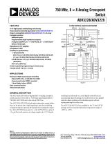
750 MHz, 8 × 8 Analog Crosspoint Switch ADV3228/ADV3229 FEATURES FUNCTIONAL BLOCK DIAGRAM SER/PAR CLK 40-BIT SHIFT REGISTER WITH 4-BIT PARALLEL LOADING 8 (RESERVED) APPLICATIONS Routing of high speed signals including Video (NTSC, PAL, S, SECAM, YUV, RGB) Compressed video (MPEG, wavelet) 3-level digital video (HDB3) Data communications Telecommunications SET INDIVIDUAL OR RESET ALL OUTPUTS TO OFF 8 × 8 high speed, nonblocking switch array Pinout and functionally equivalent to the AD8108/AD8109 Drop-in compatible with ADV3224/ADV3225 16 × 8 array Complete solution Buffered inputs Programmable high impedance outputs 8 output amplifiers, G = +1 (ADV3228), G = +2 (ADV3229) Drives 150 Ω loads Operates on ±5 V supplies Low power: 0.5 W Excellent ac performance −3 dB bandwidth 200 mV p-p: 1200 MHz (ADV3228), 900 MHz (ADV3229) 2 V p-p: 750 MHz (ADV3228), 850 MHz (ADV3229) 0.5 dB flatness (2 V p-p): 250 MHz (ADV3228), 235 MHz (ADV3229) Slew rate: 2500 V/μs Serial or parallel programming of switch array 72-lead LFCSP (10 mm × 10 mm) GENERAL DESCRIPTION The ADV3228/ADV3229 are high speed 8 × 8 analog crosspoint switch matrices. They offer a −3 dB large signal bandwidth of 750 MHz (ADV3228) and a slew rate of 2500 V/μs. The ADV3228/ADV3229 include eight independent output buffers that can be placed into a high impedance state for paralleling crosspoint outputs to prevent off channels from loading the output bus. The ADV3228 has a gain of +1, the ADV3229 has a gain of +2, and they both operate on voltage supplies of ±5 V. Channel switching is performed via a serial digital control that can accommodate daisy chaining of several devices or via a parallel control to allow updating of an individual output without reprogramming the entire array. The ADV3228/ADV3229 are available in the 72-lead LFCSP package over the extended industrial temperature range of −40°C to +85°C. Rev. 0 Information furnished by Analog Devices is believed to be accurate and reliable. However, no responsibility is assumed by Analog Devices for its use, nor for any infringements of patents or other rights of third parties that may result from its use. Specifications subject to change without notice. No license is granted by implication or otherwise under any patent or patent rights of Analog Devices. Trademarks and registered trademarks are the property of their respective owners. One Technology Way, P.O. Box 9106, Norwood, MA 02062-9106, U.S.A. Tel: 781.329.4700 www.analog.com Fax: 781.461.3113 ©2010 Analog Devices, Inc. All rights reserved.
Open the catalog to page 1
REVISION HISTORY 11/10—Revision 0: Initial Version
Open the catalog to page 2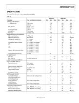
ADV3228/ADV3229 SPECIFICATIONS VS = ±5 V, TA = 25°C, RL = 150 Ω, unless otherwise noted. Table 1. Parameter DYNAMIC PERFORMANCE −3 dB Bandwidth Gain Flatness Propagation Delay Settling Time Slew Rate NOISE/DISTORTION PERFORMANCE Differential Gain Error Differential Phase Error Crosstalk, All Hostile, RTO Off Isolation, Input to Output OIP2 OIP3 Output 1 dB Compression Point Input Voltage Noise Density DC PERFORMANCE Gain Error Gain Matching Gain Temperature Coefficient OUTPUT CHARACTERISTICS Output Resistance Output Disabled Capacitance Output Leakage Current Output Voltage Range Short-Circuit...
Open the catalog to page 3
ADV3228/ADV3229 Parameter POWER SUPPLIES Supply Current Supply Voltage Range PSRR OPERATING TEMPERATURE RANGE Temperature Range θJA Test Conditions/Comments AVCC, outputs enabled, no load AVCC, outputs disabled AVEE, outputs enabled, no load AVEE, outputs disabled DVCC, outputs enabled, no load ±4.5 DC to 50 kHz, AVCC, AVEE f = 100 kHz, AVCC, AVEE f = 10 MHz, AVCC f = 10 MHz, AVEE f = 100 MHz, AVCC f = 100 MHz, AVEE f = 100 kHz, DVCC Operating (still air) Operating (still air)
Open the catalog to page 4
ADV3228/ADV3229 TIMING CHARACTERISTICS (SERIAL) Table 2. Parameter Serial Data Setup Time CLK Pulse Width Serial Data Hold Time CLK Pulse Separation, Serial Mode CLK to UPDATE Delay UPDATE Pulse Width CLK to DATAOUT Valid, Serial Mode Propagation Delay, UPDATE to Switch On or Off Data Load Time, CLK = 5 MHz, Serial Mode CLK, UPDATE Rise and Fall Times RESET Time Timing Diagram—Serial Mode t2 LOAD DATA INTO SERIAL REGISTER ON FALLING EDGE 1 = LATCHED UPDATE 0 = TRANSPARENT TRANSFER DATA FROM SERIAL REGISTER TO PARALLEL LATCHES DURING LOW LEVEL 09318-002 Figure 2. Timing Diagram, Serial Mode LOGIC...
Open the catalog to page 5
ADV3228/ADV3229 TIMING CHARACTERISTICS (PARALLEL) Table 4. Parameter Parallel Data Setup Time Address Setup Time CLK Pulse Width Parallel Data Hold Time Address Hold Time CLK Pulse Separation UPDATE Pulse Width CLK, UPDATE Rise and Fall Times RESET Time 1 = LATCHED UPDATE 0 = TRANSPARENT Figure 3. Timing Diagram, Parallel Mode
Open the catalog to page 6
ADV3228/ADV3229 ABSOLUTE MAXIMUM RATINGS POWER DISSIPATION 6V AVEE < VIN < AVCC DGND < DIN < DVCC AGND AVEE < VOUT < AVCC Momentary Internally limited to 55 mA −65°C to +125°C −40°C to +85°C 150°C 300°C Packaged in the 72-lead LFCSP, the ADV3228/ADV3229 junctionto-ambient thermal impedance (θJA) is 29°C/W. For long-term reliability, the maximum allowed junction temperature of the die should not exceed 125°C; even temporarily exceeding this limit can cause a shift in parametric performance due to a change in stresses exerted on the die by the package. Exceeding a junction temperature of 150°C...
Open the catalog to page 7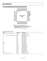
AGND NC AVEE NC AVCC NC AVEE NC AVCC NC AVEE NC AVCC NC AVEE NC AGND DVCC PIN CONFIGURATION AND FUNCTION DESCRIPTIONS DGND RESET CE DATAOUT CLK DATAIN UPDATE SER/PAR A0 A1 A2 D0 D1 D2 D3 NC DGND DVCC NOTES 1. NC = NO CONNECT. DO NOT CONNECT TO THIS PIN. 2. EXPOSED PADDLE. THE EXPOSED METAL PADDLE ON THE BOTTOM OF THE LFCSP PACKAGE MUST BE SOLDERED TO THE PCB AGND FOR PROPER HEAT DISSIPATION AND FOR NOISE AND MECHANICAL STRENGTH BENEFITS. Description Analog Positive Supply. Input Number 0. Analog Negative Supply. Input Number 1. Input Number 2. Input Number 3. Input Number 4. Input Number 5. Input...
Open the catalog to page 8All Analog Devices catalogs and technical brochures
 HMC722LP3E
8 Pages
 Isolated Sigma-Delta Modulator
17 Pages
 HMC853 Data Sheet
10 Pages
 AN-1084
8 Pages
 AN-1091
2 Pages
 AN_737
8 Pages
 AN-0982
4 Pages
 ADF7024
24 Pages
 AD9915
48 Pages
 AD9914
48 Pages
 ADRF6612
59 Pages
 ADRF6820
48 Pages
 ADL5246
32 Pages
 ADA4961
22 Pages
 AN-1141
8 Pages
 AN-698
36 Pages
 Temperature Sensors
2 Pages
 Reference Circuits
8 Pages
 Precision ADCs
16 Pages
 ADR02ACHIPS: ADR02ACHIPS
8 Pages
 AD9364 RF Agile Transceiver
32 Pages
 Digital Temperature Sensors
2 Pages
 Digital to Analog Converter ICs
12 Pages
 AD1836A: Multichannel 96 kHz Codec
24 Pages




























Archived catalogs
 Zero-Drift Amplifiers
2 Pages
 Powering ADI Components
8 Pages




- Ethernet switch
- Industrial network switch
- Acceleration sensor
- Unmanaged switch
- Analog Devices motor controller
- Transceiver module
- Triaxial acceleration sensor
- DC motor controller
- Data acquisition unit
- Analog Devices stepper motor controller
- Industrial converter
- Ethernet transceiver
- Processor
- High-voltage amplifier
- Low-noise amplifier
- Compact motor controller
- Digital converter
- Closed-loop motor controller
- Digital motor controller