
- Catalogs
- Analog Devices
- ADSP-CM402F/CM403F/CM407F/CM408F/CM409F: Mixed-Signal Control Processor with ARM Cortex-M4 and 16-bit ADCs


- Products
- Catalogs
- News & Trends
- Exhibitions
ADSP-CM402F/CM403F/CM407F/CM408F/CM409F: Mixed-Signal Control Processor with ARM Cortex-M4 and 16-bit ADCs
ADSP-CM402F/CM403F/CM407F/CM408F/CM409F: Mixed-Signal Control Processor with ARM Cortex-M4 and 16-bit ADCs
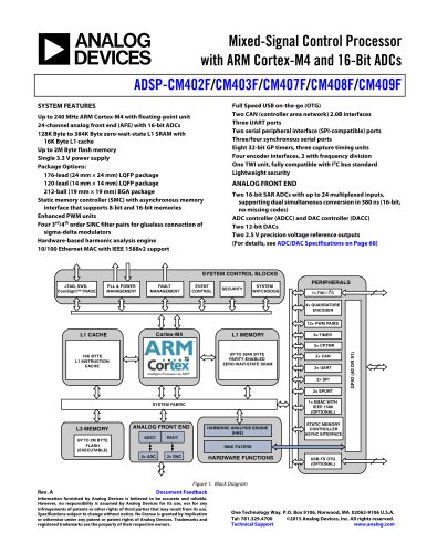
The ADSP-CM40xF family of mixed-signal control processors is based on the ARM Cortex-M4 processor core with a floating-point unit, operating at frequencies up to 240 MHz. It integrates up to 384 kB of SRAM memory, 2 MB of flash memory, and peripherals optimized for motor control and photovoltaic inverter control. The analog module includes two 16-bit SAR ADCs and two 12-bit DACs. These processors are designed for low power consumption and are suitable for applications in power/motor control, embedded industrial, instrumentation, medical, and consumer markets.
The processors feature up to 240 MHz ARM Cortex-M4, a 24-channel analog front end with 16-bit ADCs, and up to 2M Byte flash memory. They support a single 3.3 V power supply and offer various package options. Key peripherals include enhanced PWM units, Ethernet MAC with IEEE 1588v2 support, USB OTG, CAN interfaces, UART ports, SPI-compatible ports, and more.
The analog front end consists of two 16-bit SAR ADCs and two 12-bit DACs, managed by an ADC controller (ADCC) and a DAC controller (DACC). The ADCC supports dual simultaneous sampling and can deliver 16 channels of ADC data to memory in 3 μs. The DACC interfaces with the DACs for efficient management. The ADC module allows conversion of up to 26 analog input sources, with a voltage input range from 0 V to 2.5 V.
The processors include up to 384K Byte zero-wait-state L1 SRAM with 16K Byte L1 cache and up to 2M Byte flash memory. The static memory controller supports 8-bit and 16-bit memories.
The processors offer lightweight security features and reliability enhancements, including watchdog timers and fault management systems.
Development tools and additional technical support are available through Analog Devices' website. Detailed signal descriptions and specifications are provided in the document for various processor models.
The document outlines a typical power supply configuration for the ADSP-CM40xF series, highlighting the use of ceramic capacitors and low ESR capacitors for stability and performance.
The ARM Cortex-M4 core is a 32-bit RISC processor with features such as Thumb-2 ISA technology, DSP and SIMD extensions, a single-precision FPU, and a comprehensive debug and trace system. It supports low power configurations and includes an EmbeddedICE module for debugging.
Key components include DMA controllers, a System Event Controller for fault management, a Trigger Routing Unit for system-level control, and Pin Interrupts for flexible interrupt management. The GPIO system supports multiplexing with various peripherals.
The processor includes a Harmonic Analysis Engine for power quality measurements and a Sinus Cardinalis Filter for noise reduction and enhanced signal processing.
Features designed to enhance the robustness of system safety and reliability include multi-parity-bit protection for L1 memories, a Cortex MPU for memory management, and a System Protection Unit (SPU) for controlling access to system resources. Watchpoint protection and software watchdogs are also implemented to monitor system activities and ensure stability.
Various watchdog mechanisms are described, including signal watchdogs for monitoring off-chip signals, an oscillator watchdog for clock oscillator monitoring, and low-latency sinc filter over-range detection for ADC bitstream monitoring. These mechanisms help detect and manage system faults effectively.
The fault management unit within the system event controller (SEC) can define system events as faults, potentially resetting the device or signaling off-chip hardware. It provides a delay mechanism for fault actions, allowing the core to resolve issues before actions are taken.
The processor includes a variety of peripherals connected via high-bandwidth buses, enhancing system configuration flexibility and performance. These peripherals include timers, watchdog timers, capture timers, PWM units, serial ports, general-purpose counters, SPI ports, UART ports, TWI interfaces, CAN controllers, and Ethernet MACs.
The document outlines the features of a processor supporting RMII protocols for external PHYs, full-duplex and half-duplex modes, media access management, flow control, and station management for PHY register access. Advanced features include automatic checksum computation, independent DMA channels, frame status delivery, and advanced power management. It supports 802.3Q VLAN frames and IEEE 1588 for precision clock synchronization.
The processor includes hardware support for IEEE 1588, providing precision time protocol synchronization with features like 64-bit time stamping, PTP message identification, and multiple input clock sources.
This controller offers connectivity for industrial applications and consumer devices, supporting both peripheral and host modes.
The processor has three operating modes with different power profiles, utilizing an external crystal or on-chip oscillator for clocking. It includes a programmable oscillator watchdog and a clock generation unit (CGU) for managing on-chip clocks.
The processor supports dynamic power management, allowing control over the core clock frequency to reduce power consumption. It operates across three power domains: VDD_INT, VDD_EXT, and VDD_ANA.
The RCU manages how functional units enter and exit reset, with hardware and system reset options.
Features include JTAG and Serial Wire Debug Port (SWJ-DP), Embedded Trace Macrocell (ETM), and Instrumentation Trace Macrocell (ITM) for debugging.
The processor is supported by development tools for embedded applications, with additional documentation available from Analog Devices.
Signal chains are used in signal processing applications, with tools available for viewing relationships between applications and components on the Analog Devices website.
The document provides detailed signal descriptions and multiplexing information for the ADSP-CM402F/CM403F/CM407F/CM408F/CM409F processors, specifically focusing on the 120-lead and 176-lead LQFP packages. It includes specifications for various signal nodes, their functions, and recommended configurations.
- Signal Descriptions: The document lists signal names, descriptions, ports, and pin names for both 120-lead and 176-lead LQFP packages. Each signal is described in terms of its function and whether it is multiplexed or not.
- Power Regulation Bypass Nodes: Details on on-chip analog and digital power regulation bypass filter nodes for ADCs and the analog subsystem are provided, with references to recommended bypass configurations in Figure 4 on Page 6.
- CAN and UART Interfaces: Descriptions of CAN and UART signal functions, including receive and transmit capabilities, are outlined with their respective port and pin assignments.
- GPIO Multiplexing: Tables 8 through 10 detail the multiplexing of general-purpose I/O pins for the 120-lead LQFP package, showing multiple functions for each pin and their input taps.
- Ethernet and Timer Functions: The document includes descriptions of Ethernet MAC (EMAC) signals and various timer functions, highlighting their roles and pin assignments.
- Bypass Recommendations: Several signals require specific bypass configurations as recommended in Figure 4 on Page 6, crucial for optimal performance.
- Multiplexing Details: Understanding the multiplexing of GPIO pins is essential for configuring the processor correctly in different applications.
- Signal Functionality: Each signal's role, whether for communication, power regulation, or data processing, is critical for system design and integration.
- Transient duty cycle applies to 100% unless specified otherwise. For other duty cycles, refer to Table 32.
- TWI Digital Input Voltage ranges from -0.33 V to +3.63 V, applicable to pins TWI_SCL and TWI_SDA.
- Digital Output Voltage Swing is from -0.33 V to VDD_EXT + 0.5 V.
- Analog Input Voltage is specified as -0.33 V to +3.63 V when VDD_ANA is within specification.
- USB0_Dx Input Voltage ranges from -0.33 V to +5.25 V.
- Maximum IOH/IOL Current per Signal is 6 mA.
- Storage Temperature Range is from -65°C to +150°C.
- Table 32 outlines the maximum duty cycle for input transient voltage, with specific voltage ranges for different duty cycles.
- The document provides package brand information and highlights the importance of ESD precautions due to the sensitivity of the device.
- Clock and Reset Timing: SYS_CLKIN frequency ranges from 20 to 60 MHz depending on the mode, with specific pulse width requirements.
- Power-Up Reset Timing: Describes the relationship between power supply startup and processor reset timing.
- Asynchronous Read and Write: Detailed timing requirements for asynchronous memory operations, including setup, hold, and delay times.
- Asynchronous Flash Read and Write: Similar timing specifications for flash memory operations.
- Specifications for serial port communication, including frame sync, data setup, and hold times for both external and internal clock configurations.
- Detailed timing for enabling and disabling data transmission in multichannel mode.
The document provides detailed timing specifications for the 10/100 Ethernet MAC Controller, focusing on RMII receive and transmit signals, and station management. Key parameters include the period and width of the reference clock (tREFCLKEXT), setup and hold times for data input and output, and switching characteristics.
The SINC filter timing section outlines the setup and hold requirements for the SINC0_Dx signals relative to the SINC0_CLKx rise. It also specifies the programmable clock period (tSINCLKPROG) and its width.
This section covers the timing for trace operations and the Serial Wire Debug (SWD) interface, including setup, hold, and delay times for data relative to clock signals. The JTAG emulation port timing is also detailed, with specific requirements for setup and hold times for various signals.
The document describes the conditions under which timing parameters are measured, including output enable and disable times, and the impact of capacitive loading on timing.
Thermal characteristics for different package types (120-Lead LQFP, 176-Lead LQFP, 212-Ball BGA) are provided, including junction-to-ambient and junction-to-case thermal resistances, which are crucial for thermal management in design.
Detailed lead assignments for the 120-lead and 176-lead LQFP packages are provided, both numerically and alphabetically, to assist in proper pin configuration and connection.
Catalog excerpts
Mixed-Signal Control Processor with ARM Cortex-M4 and 16-Bit ADCs ADSP-CM402F/CM403F/CM407F/CM408F/CM409F SYSTEM FEATURES Full Speed USB on-the-go (OTG) Two CAN (controller area network) 2.0B interfaces Three UART ports Two serial peripheral interface (SPI-compatible) ports Three/four synchronous serial ports Eight 32-bit GP timers, three capture timing units Four encoder interfaces, 2 with frequency division One TWI unit, fully compatible with I2C bus standard Lightweight security Up to 240 MHz ARM Cortex-M4 with floating-point unit 24-channel analog front end (AFE) with 16-bit ADCs 128K Byte to 384K Byte zero-wait-state L1 SRAM with 16K Byte L1 cache Up to 2M Byte flash memory Single 3.3 V power supply Package Options: 176-lead (24 mm × 24 mm) LQFP package 120-lead (14 mm × 14 mm) LQFP package 212-ball (19 mm × 19 mm) BGA package Static memory controller (SMC) with asynchronous memory interface that supports 8-bit and 16-bit memories Enhanced PWM units Four 3rd/4th order SINC filter pairs for glueless connection of sigma-delta modulators Hardware-based harmonic analysis engine 10/100 Ethernet MAC with IEEE 1588v2 support ANALOG FRONT END Two 16-bit SAR ADCs with up to 24 multiplexed inputs, supporting dual simultaneous conversion in 380 ns (16-bit, no missing codes) ADC controller (ADCC) and DAC controller (DACC) Two 12-bit DACs Two 2.5 V precision voltage reference outputs (For details, see ADC/DAC Specifications on Page 68) SYSTEM CONTROL BLOCKS JTAG, SWD, CoreSight™ TRACE FAULT MANAGEMENT EVENT CONTROL SYSTEM WATCHDOGS 4× QUADRATURE ENCODER 12× PWM PAIRS 16K BYTE L1 INSTRUCTION CACHE 3× CPTMR UP TO 384K BYTE PARITY-ENABLED ZERO-WAIT-STATE SRAM 2x SPORT 1× EMAC WITH IEEE 1588 (OPTIONAL) SYSTEM FABRIC L3 MEMORY UP TO 2M BYTE FLASH (EXECUTABLE) ANALOG FRONT END ADCC STATIC MEMORY CONTROLLER ASYNC INTERFACE HARMONIC ANALYSIS ENGINE (HAE) HARDWARE FUNCTIONS Figure 1. Block Diagram Document Feedback Information furnished by Analog Devices is believed to be accurate and reliable. However, no responsibility is assumed by Analog Devices for its use, nor for any infringements of patents or other rights of third parties that may result from its use. Specifications subject to change without notice. No license is granted by implication or otherwise under any patent or patent rights of Analog Devices. Trademarks and registered trademarks are the property of their respective owners. One Technology Way, P.O. Box 9106, Norwood, MA 02062-9106 U.S.A. Tel: 781.329.4700 ©2015 Analog Devices, Inc. All rights reserved. Technical Support www.analog.com
Open the catalog to page 1
ADSP-CM402F/CM403F/CM407F/CM408F/CM409F GENERAL DESCRIPTION Each ADSP-CM40xF family member contains the following modules. The ADSP-CM40xF family of mixed-signal control processors is based on the ARM® Cortex-M4TM processor core with floatingpoint unit operating at frequencies up to 240 MHz and integrating up to 384 kB of SRAM memory, 2 MB of flash memory, accelerators and peripherals optimized for motor control and photo-voltaic (PV) inverter control and an analog module consisting of two 16-bit SAR ADCs and two 12-bit DACs. The ADSP-CM40xF family operates from a single voltage supply (VDD_EXT/VDD_ANA),...
Open the catalog to page 3
ADSP-CM402F/CM403F/CM407F/CM408F/CM409F ANALOG FRONT END The mixed-signal controllers contain two ADCs and two DACs. Control of these data converters is simplified by a powerful onchip analog-to-digital conversion controller (ADCC) and a digital-to-analog conversion controller (DACC). The ADCC and DACC are integrated seamlessly into the software programming model, and they efficiently manage the configuration and realtime operation of the ADCs and DACs. simultaneously or at different times and may be operated in asynchronous or synchronous modes. The best performance can be achieved in synchronous...
Open the catalog to page 4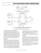
ADCC CONTROL SRAM MEMORY DATA ADC/DAC LOCAL CONTROLLER DAC0 VREF0 VREF1 REFCAP NOTE: DAC0 AND DAC1 CAN BE MUX SELECTED THROUGH AN INTERNAL PATH WITHIN THE CHIP. SEE THE HARDWARE REFERENCE MANUAL FOR PROGRAMMING DETAIL. Figure 3. ADSP-CM407F/ADSP-CM408F Analog Subsystem Block Diagram Considerations for Best Converter Performance As with any high performance analog/digital circuit, to achieve best performance, good circuit design and board layout practices should be followed. The power supply and its noise bypass (decoupling), ground return paths and pin connections, and analog/digital routing...
Open the catalog to page 5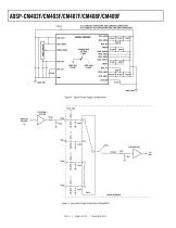
ADSP-CM402F/CM403F/CM407F/CM408F/CM409F ALL LABELED CAPACITORS ARE CERAMIC CAPACITORS. ALL LABELED 10μF CAPACITORS ARE LOW ESR CAPACITORS. VREG CIRCUIT VDD_INT GND_DIG PLANE GND_ANA PLANE Figure 4. Typical Power Supply Configuration VDD_ANA EXTERNAL BUFFER ANALOG SOURCE HOLD PRE-BUFFER TRACK Figure 5. Equivalent Single-Ended Input (Simplified)
Open the catalog to page 6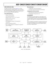
Microarchitecture • 3-stage pipeline with branch speculation The ARM Cortex-M4, core shown in Figure 6, is a 32-bit reduced instruction set computer (RISC). It uses 32-bit buses for instruction and data. The length of the data can be 8 bits, 16 bits, or 32 bits. The length of the instruction word is 16 or 32 bits. The controller has the following features. • Low-latency interrupt processing with tail chaining Configurable For Ultra Low Power • Deep sleep mode, dynamic power management • Programmable clock generator unit EmbeddedICETM provides integrated on-chip support for the core. The EmbeddedICE...
Open the catalog to page 7
• GPIO interrupt mask registers—Allow each individual GPIO pin to function as an interrupt to the processor. GPIO pins defined as inputs can be configured to generate hardware interrupts, while output pins can be triggered by software interrupts. The processor contains 17 independent and concurrently operating peripheral DMA channels plus two MDMA streams. DDE Channel 0 to Channel 16 are for peripherals and Channel 17 to Channel 20 are for MDMA. • GPIO interrupt sensitivity registers—Specify whether individual pins are level- or edge-sensitive and specify—if edge-sensitive—whether just the rising...
Open the catalog to page 8All Analog Devices catalogs and technical brochures
 HMC722LP3E
8 Pages
 Isolated Sigma-Delta Modulator
17 Pages
 HMC853 Data Sheet
10 Pages
 AN-1084
8 Pages
 AN-1091
2 Pages
 AN_737
8 Pages
 AN-0982
4 Pages
 ADF7024
24 Pages
 AD9915
48 Pages
 AD9914
48 Pages
 ADRF6612
59 Pages
 ADRF6820
48 Pages
 ADL5246
32 Pages
 ADA4961
22 Pages
 AN-1141
8 Pages
 AN-698
36 Pages
 Temperature Sensors
2 Pages
 Reference Circuits
8 Pages
 Precision ADCs
16 Pages
 ADR02ACHIPS: ADR02ACHIPS
8 Pages
 AD9364 RF Agile Transceiver
32 Pages
 Digital Temperature Sensors
2 Pages
 Digital to Analog Converter ICs
12 Pages
 AD1836A: Multichannel 96 kHz Codec
24 Pages




























Archived catalogs
 Zero-Drift Amplifiers
2 Pages
 Powering ADI Components
8 Pages




- Ethernet switch
- Industrial network switch
- Acceleration sensor
- Unmanaged switch
- Analog Devices motor controller
- Transceiver module
- Triaxial acceleration sensor
- DC motor controller
- Data acquisition unit
- Analog Devices stepper motor controller
- Industrial converter
- Ethernet transceiver
- High-voltage amplifier
- Low-noise amplifier
- Multiplexer
- Compact motor controller
- Digital converter
- Closed-loop motor controller
- Digital motor controller
- VirtualExpo Group
- Our Partners
- Recruitment
- Testimonials