- Catalogs
- Analog Devices
- ADRF6820
ADRF6820
1 /48Pages

ADRF6820
1 /48Pages
Catalog excerpts

695 MHz to 2700 MHz, Quadrature Demodulator with Integrated Fractional-N PLL and VCO Data Sheet SCLK FUNCTIONAL BLOCK DIAGRAM DC/PHASE CORRECTION SERIAL PORT INTERFACE POLYPHASE FILTER I/Q demodulator with integrated fractional-N PLL RF input frequency range: 695 MHz to 2700 MHz Internal LO frequency range: 356.25 MHz to 2850 MHz Input P1dB: 14.5 dBm at 1900 MHz RF Input IP3: 35 dBm at 1900 MHz RF Programmable HD3/IP3 trim Single pole, double throw (SPDT) RF input switch RF digital step attenuation range: 0 dB to 15 dB Integrated RF tunable balun for single-ended 50 Ω input Multicore integrated VCO Demodulated 1 dB bandwidth: 600 MHz 4 selectable baseband gain and bandwidth modes Digital programmable LO phase offset and dc nulling Programmable via 3-wire serial port interface (SPI) 40-lead, 6 mm × 6 mm LFCSP APPLICATIONS Cellular W-CDMA/GSM/LTE Digital predistortion (DPD) receivers Microwave point-to-point radios GENERAL DESCRIPTION The ADRF6820 is a highly integrated demodulator and synthesizer ideally suited for next generation communication systems. The feature rich device consists of a high linearity broadband I/Q demodulator, an integrated fractional-N phase-locked loop (PLL), and a low phase noise multicore, voltage controlled oscillator (VCO). The ADRF6820 also integrates a 2:1 RF switch, an on-chip tunable RF balun, a programmable RF attenuator, and two low dropout (LDO) regulators. This highly integrated device fits within a small 6 mm × 6 mm footprint. The high isolation 2:1 RF switch and on-chip tunable RF balun enable the ADRF6820 to support two single-ended, 50 Ω terminated RF inputs. A programmable attenuator ensures an optimal differential RF input level to the high linearity demodulator core. The integrated attenuator offers an attenuation range of 0 dB to 15 dB with a step size of 1 dB. The ADRF6820 offers two alternatives for generating the differential local oscillator (LO) input signal: externally via a high frequency, low phase noise LO signal or internally via the on-chip fractional-N synthesizer. The integrated synthesizer enables continuous LO coverage from 356.25 MHz to 2850 MHz. The PLL reference input can support a wide frequency range because the divide or multiplication blocks can increase or decrease the reference frequency to the desired value before it is passed to the phase frequency detector (PFD). When selected, the output of the internal fractional-N synthesizer is applied to a divide-by-2 quadrature phase splitter. From the external LO path, a 1× LO signal can be applied to the built-in polyphase filter, or a 2× LO signal can be used with the divideby-2 quadrature phase splitter to generate the quadrature LO inputs to the mixers. The ADRF6820 is fabricated using an advanced silicon-germanium BiCMOS process. It is available in a 40-lead, RoHS-compliant, 6 mm × 6 mm LFCSP package with an exposed paddle. Performance is specified over the −40°C to +85°C temperature range. Document Feedback Information furnished by Analog Devices is believed to be accurate and reliable. However, no responsibility is assumed by Analog Devices for its use, nor for any infringements of patents or other rights of third parties that may result from its use. Specifications subject to change without notice. No license is granted by implication or otherwise under any patent or patent rights of Analog Devices. Trademarks and registered trademarks are the property of their respective owners. One Technology Way, P.O. Box 9106, Norwood, MA 02062-9106, U.S.A. Tel: 781.329.4700 ©2013–2014 Analog Devices, Inc. All rights reserved. Technical Support www.analog.com
Open the catalog to page 1
Data Sheet
Open the catalog to page 2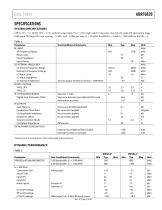
Data Sheet SPECIFICATIONS SYSTEM SPECIFICATIONS VPOS_5V = 5 V, VPOS_3P3 = 3.3 V, ambient temperature (TA) = 25°C, high-side LO injection, internal LO mode, RF attenuation range = 0 dB, input IP2/input IP3 tone spacing = 5 MHz and −5 dBm per tone, fIF = 40 MHz for BWSEL = 0 and fIF = 200 MHz for BWSEL = 2. Table 1. Parameter RF INPUT RF Frequency Range Return Loss Input Impedance Input Power LO INTERNAL FREQUENCY LO Internal Frequency Range External LO Frequency Range LO Input Level LO Input Impedance LO Harmonic Rejection 1 SUPPLY VOLTAGE VPOS_3P3 VPOS_5V RF ATTENUATION RANGE Digital Step Attenuator...
Open the catalog to page 3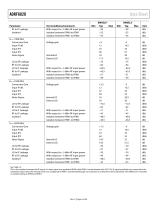
ADRF6820 Parameter RF to IF Leakage Isolation 2 fRF = 1900 MHz Conversion Gain Input P1dB Input IP3 Input IP2 Noise Figure LO to RF Leakage RF to LO Leakage LO to IF Leakage RF to IF Leakage Isolation2 fRF = 2100 MHz Conversion Gain Input P1dB Input IP3 Input IP2 Noise Figure LO to RF Leakage RF to LO Leakage LO to IF Leakage RF to IF Leakage Isolation2 fRF = 2650 MHz Conversion Gain Input P1dB Input IP3 Input IP2 Noise Figure LO to RF Leakage RF to LO Leakage LO to IF Leakage RF to IF Leakage Isolation2 1 2 Data Sheet Test Conditions/Comments With respect to −5 dBm RF input power Isolation between...
Open the catalog to page 4
Data Sheet SYNTHESIZER/PLL SPECIFICATIONS VPOS_5V = 5 V, VPOS_3P3 = 3.3 V, ambient temperature (TA) = 25°C, fREF = 153.6 MHz, fREF power = 4 dBm, fPFD = 38.4 MHz, loop filter bandwidth = 20 kHz, measured at LO output, Table 3. Parameter PLL REFERENCE Frequency Amplitude PLL Step Size 1 PLL Lock Time 2 PFD FREQUENCY INTERNAL VCO RANGE REFERENCE SPURS INTEGRATED PHASE NOISE 3 CLOSED-LOOP PERFORMANCE 20 kHz Loop Filter Test Conditions/Comments 12 PFD = 30.72 MHz PFD = 30.72 MHz, charge pump = 500 µA, loop bandwidth = 40 kHz, antibacklash delay = 0.5 ns, charge pump bleed current = 78.125 µA down...
Open the catalog to page 5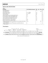
Data Sheet DIGITAL LOGIC SPECIFICATIONS Table 4. Parameter Input Voltage High, VIH Input Voltage Low, VIL Output Voltage High, VOH Output Voltage Low, VOL Serial Clock Period Setup Time Between Data and Rising Edge of SCLK Hold Time Between Data and Rising Edge of SCLK Setup Time Between Falling Edge of CS and SCLK Hold Time Between Rising Edge of CS and SCLK Minimum Period SCLK in a Logic High State Minimum Period SCLK in a Logic Low State Maximum Time Delay Between Falling Edge of SCLK and Output Data Valid for a Read Operation Maximum Time Delay Between CS Deactivation and SDIO Bus Return...
Open the catalog to page 6All Analog Devices catalogs and technical brochures
 HMC722LP3E
8 Pages
 Isolated Sigma-Delta Modulator
17 Pages
 HMC853 Data Sheet
10 Pages
 AN-1084
8 Pages
 AN-1091
2 Pages
 AN_737
8 Pages
 AN-0982
4 Pages
 ADF7024
24 Pages
 AD9915
48 Pages
 AD9914
48 Pages
 ADRF6612
59 Pages
 ADL5246
32 Pages
 ADA4961
22 Pages
 AN-1141
8 Pages
 AN-698
36 Pages
 Temperature Sensors
2 Pages
 Reference Circuits
8 Pages
 Precision ADCs
16 Pages
 ADR02ACHIPS: ADR02ACHIPS
8 Pages
 AD9364 RF Agile Transceiver
32 Pages
 Digital Temperature Sensors
2 Pages
 Digital to Analog Converter ICs
12 Pages
 AD1836A: Multichannel 96 kHz Codec
24 Pages


Archived catalogs
 Zero-Drift Amplifiers
2 Pages
 Powering ADI Components
8 Pages


- Ethernet switch
- Industrial network switch
- Acceleration sensor
- Unmanaged switch
- Transceiver module
- Analog Devices motor controller
- Triaxial acceleration sensor
- DC motor controller
- Data acquisition unit
- Analog Devices stepper motor controller
- Industrial converter
- Ethernet transceiver
- Processor
- High-voltage amplifier
- Low-noise amplifier
- Multiplexer
- Compact motor controller
- Gyroscope
- Closed-loop motor controller
- Digital converter