
- Catalogs
- Analog Devices
- ADRF6612


- Products
- Catalogs
- News & Trends
- Exhibitions
ADRF6612

ADRF6612
The ADRF6612 is a dual passive receive mixer with an integrated PLL and VCO, operating over an RF frequency range of 700 MHz to 3000 MHz. It supports LO frequencies from 200 MHz to 2700 MHz and IF ranges from 40 to 500 MHz. Key performance metrics include a power conversion gain of 9.2 dB, an SSB noise figure of 11.3 dB, and an input IP3 of 28 dBm. The device is housed in a 7 x 7 mm, 48-lead LFCSP package.
This mixer is suitable for multi-band/multi-standard cellular base station diversity receivers, wideband radio link diversity downconverters, and multi-mode cellular extenders and picocells.
The ADRF6612 features a dual RF mixer and IF amplifier with integrated PLL and VCO, utilizing broadband square wave limiting LO amplifiers for a wide RF bandwidth. It employs highly linear doubly balanced passive mixer cores with integrated RF and LO balancing circuits, allowing for single-ended operation. The device supports both integer-N and fractional-N PLL operation, with an external reference input frequency range of 12 MHz to 320 MHz.
In high performance mode, the device offers a tunable RF return loss greater than 20 dB, an RF frequency range of 700 to 3000 MHz, and an IF frequency range of 40 to 500 MHz. The power conversion gain is 9.2 dB, with a voltage conversion gain of 15.2 dB. The input third-order intercept point is 29 dBm, and the input 1 dB compression point is 11.5 dBm.
In integer mode, the synthesizer supports an LO frequency range of 200 to 2700 MHz, with a phase noise figure of merit of -222 dBc/Hz. The charge pump current is programmable up to 8 mA, with an output compliance range of 1 to 2.8 V. In fractional mode, similar specifications apply, with a focus on reducing fractional spurs using a sigma-delta modulator.
An evaluation board is available for testing and development. The device operates over a temperature range of -40°C to +85°C, with considerations for thermal resistance and junction temperature management.
1. Reference Input: Input capacitance is 4 pF. Reference divider value ranges from 0.5 to 2047.
2. MUXOUT Output: Output levels are 0.25 V (VOL) and 2.7 V (VOH) with a 50% duty cycle.
3. VCO Phase Noise (Locked): Detailed phase noise values are provided for VCO_0 to VCO_3 at various offsets, with integrated phase noise ranging from 0.4 to 0.6 °rms.
4. VCO Phase Noise (Open Loop): Phase noise values are given for VCO_0 to VCO_3 at different frequencies and offsets.
1. Logic Inputs: High voltage (VINH) is 1.4 to 3.3 V, low voltage (VINL) is 0 to 0.7 V, with an input current of 0.1 μA and capacitance of 5 pF.
2. Power Supplies: Voltage range for high performance mode is 4.75 to 5.25 V, and for high efficiency mode is 3.45 to 3.75 V. Power dissipation varies based on mode and external LO output status.
1. Input/Output Voltages: VIH is 1.4 V, VIL is 0.70 V, VOH is 2.3 V, and VOL is 0.2 V.
2. Timing: Various setup and hold times are specified for SCLK and CSB signals.
1. Voltage Ratings: Supply voltage ranges from -0.5 V to +5.5 V, and digital I/O from -0.3 V to +3.6 V.
2. Temperature Ratings: Operating range is -40°C to +85°C, with a maximum junction temperature of 150°C.
1. Package Type: LFCSP48 with a thermal resistance of 3.0 °C/W.
1. Pin Descriptions: Detailed descriptions are provided for each pin, including power supply, ground connections, and signal inputs/outputs.
1. High Performance Mode: Graphs illustrate power dissipation, conversion gain, and noise figures across various frequencies and temperatures.
2. High Efficiency Mode: Similar performance characteristics are provided for this mode.
1. VCO Phase Noise: Open-loop and closed-loop phase noise characteristics are detailed for various VCO frequencies and divider settings.
The ADRF6612 mixer gain can be optimized by adjusting BAL_CIN and BAL_COUT values. At lower frequencies, higher capacitance is needed, while at higher frequencies, lower capacitance is sufficient. Figures illustrate gain variations at different RF frequencies.
The ADRF6612 allows for IIP3 optimization by adjusting the IF amplifier bias current, balancing performance and power consumption. Figures show IIP3 sweeps for various IFA Main Bias and Linearity Bias combinations at IF frequencies.
The document provides a detailed register summary for the ADRF6612, including register names, bit descriptions, settings, and access types. Key registers include SOFT_RESET, ENABLES, INT_DIV, FRAC_DIV, MOD_DIV, IF_BIAS, CP_CTRL, PFD_CTRL1, VCO_CTRL1, and others, each with specific functions and default reset values.
An evaluation board for the ADRF6612 is available, with schematics for the main circuitry and USB interface provided. The board uses Rogers® 3003 material, and the software is accessible on the Analog Devices website.
Catalog excerpts
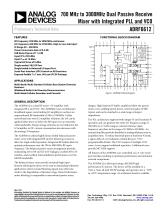
Lock Detect Multi-Band/ Multi-Standard Cellular Base Station Diversity Receivers Wideband Radio Link Diversity Downconverters Multi-Mode Cellular Extenders and Picocells EXPOSED PADDLE FUNCTIONAL BLOCK DIAGRAM RF Frequency 700 MHz to 3000 MHz continuous LO Frequency 200 MHz to 2700 MHz, High or Low side Inject IF Range 40 – 500 MHz Power Conversion Gain of 9.2 dB SSB Noise Figure of 11.3 dB Input IP3 of 28 dBm Input P1dB of 10 dBm Typical LO Drive of 0 dBm Single-ended, 50 RF Port Single Ended or Balanced LO Input Port Serial Port Interface (SPI) Control on All Functions Exposed Paddle 7 x 7 mm, 48 Lead LFCSP Package Preliminary Technical Data 700 MHz to 3000MHz Dual Passive Receive Mixer with Integrated PLL and VCO ADRF6612 Figure 1. ADRF6612 Block Diagram GENERAL DESCRIPTION The ADRF6612 is a dual RF mixer + IF amplifier with integrated PLL and VCO. The ADRF6612 uses revolutionary broadband square wave limiting LO amplifiers to achieve an unprecedented RF bandwidth of 700 to 2700MHz. Unlike narrowband sine wave LO amplifier solutions, the LO can be applied either above or below the RF input over an extremely wide bandwidth. Energy storage elements are not utilized in the LO amplifier so DC current consumption also decreases with decreasing LO frequency. The ADRF6612 utilizes highly linear doubly balanced passive mixer cores with integrated RF and LO balancing circuits to allow for single-ended operation. Integrated RF baluns allow for optimal performance over the 700 to 3000 MHz RF input frequency. The balanced passive mixer arrangement provides outstanding LO to RF and LO to IF leakages, excellent RF to IF isolation, and excellent intermodulation performance over the full RF bandwidth. The balanced mixer cores provide extremely high input linearity allowing the device to be used in demanding wideband applications where in-band blocking signals may otherwise result in the degradation of dynamic range. Noise Performance under blocking is comparable to narrowband passive mixer designs. High linearity IF buffer amplifiers follow the passive mixer cores, yielding typical power conversion gains of 9dB typical, and can be matched to a wide range of output impedances. The PLL architecture supports both integer-N and fractional-N operation and can generate the entire LO frequency range of 200 MHz to 2.7 GHz using an external reference input frequency anywhere in the range of 12 MHz to 320 MHz. An external loop filter provides flexibility in trading off phase noise vs. acquisition time. To reduce fractional spurs in fractional-N mode, a sigma-delta (Σ-Δ) modulator controls the post- VCO programmable divider. The VCO consists of multiple VCO cores. 4 cores support wideband operation. 2 additional cores provide MC-GSM support. All features of the ADRF6612 are controlled via a 3-wire serial port interface resulting in optimum performance and minimum external components. The ADRF6612 is fabricated using a BiCMOS high performance IC process. The device will be available in a 7mm x 7mm 48-lead LFCSP package and operates over a −40°C to +85°C temperature range. An evaluation board is available. Rev. PrA Information furnished by Analog Devices is believed to be accurate and reliable. However, no responsibility is assumed by Analog Devices for its use, nor for any infringements of patents or other rights of third parties that may result from its use. Specifications subject to change without notice. No license is granted by implication or otherwise under any patent or patent rights of Analog Devices. Trademarks and registered trademarks are the property of their respective owners. One Technology Way, P.O. Box 9106, Norwood, MA 02062-9106, U.S.A. Tel: 781.329.4700 www.analog.com Fax: 781.461.3113 ©2014 Analog Devices, Inc. All rights reserved.
Open the catalog to page 1
Preliminary Technical Data REVISION HISTORY
Open the catalog to page 2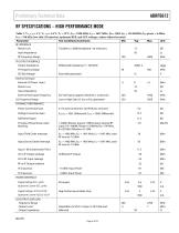
Preliminary Technical Data RF SPECIFICATIONS – HIGH PERFORMANCE MODE Table 1. VS _IF, LO= 5 V, VS _SYN= 3.6 V, TA = 25C, fRF = 1900 MHz, fLO = 1697 MHz, Zo = 50, fREF = 122.88MHz; fREF power = 4 dBm; fPFD = 768 kHz; low-side LO injection, optimum RFB, and LPF settings; unless otherwise noted Parameter RF INTERFACE Return Loss Test Conditions/Comments Tunable to >20dB broadband via serial port Externally generated External LO Input External LO Power Input Return Loss Ext VCO Input supports divide by 1,2,4,8,16,32 Low or High Side LO, Int. or Ext. generated Input Impedance LO Frequency Range External...
Open the catalog to page 3
Preliminary Technical Data RF SPECIFICATIONS – HIGH EFFICIENCY MODE Table 2. VS _IF, LO= 3.6 V, VS _SYN= 3.6 V TA = 25C, fRF = 1900 MHz, fLO = 1697 MHz, Zo = 50, fREF = 153.6 MHz; fREF power = 4 dBm; fPFD = 1.6 MHz; low-side LO injection, optimum RFB, and LPF settings; unless otherwise noted Parameter RF INTERFACE Return Loss Test Conditions/Comments Tunable to >20dB broadband via serial port Externally generated External VCO Input External VCO Power Input Return Loss Ext VCO Input supports divide by 1,2,4,8,16,32 Low or High Side LO, Int. or Ext. generated Input Impedance LO Frequency Range...
Open the catalog to page 4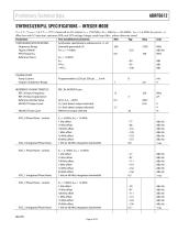
Preliminary Technical Data SYNTHESIZER/PLL SPECIFICATIONS – INTEGER MODE VS = 5 V , VSYNTH = 3.6 V TA = 25C, measured on LO output, fLO = 1700 MHz, Zo = 50, fREF =153.6MHz, fPFD = 1.6 MHz; fREF power = 4 dBm; low-side LO injection, optimum RFB, and LPF settings; Integer mode loop filter, unless otherwise noted Parameter SYNTHESIZER SPECIFICATIONS Frequency Range Figure of Merit3 PFD Frequency Reference Spurs CHARGE PUMP Pump Current Output Compliance Range REFERENCE CHARACTERISTICS REF_IN Input Frequency REF_IN Input Capacitance Reference Divider Value MUXOUT Output Level MUXOUT Duty Cycle VCO_0...
Open the catalog to page 5
ADRF6612 Parameter VCO_3 Phase Noise - Locked VCO_3 Integrated Phase Noise Preliminary Technical Data Test Conditions/Comments fLO = 1.6GHz, fPFD = 1.6 MHz 1 kHz offset 10 kHz offset 100 kHz offset 1 MHz offset 10 MHz offset 40 MHz offset 1 kHz to 40 MHz integration bandwidth Unit dBc/Hz dBc/Hz dBc/Hz dBc/Hz dBc/Hz dBc/Hz rms
Open the catalog to page 6All Analog Devices catalogs and technical brochures
 HMC722LP3E
8 Pages
 Isolated Sigma-Delta Modulator
17 Pages
 HMC853 Data Sheet
10 Pages
 AN-1084
8 Pages
 AN-1091
2 Pages
 AN_737
8 Pages
 AN-0982
4 Pages
 ADF7024
24 Pages
 AD9915
48 Pages
 AD9914
48 Pages
 ADRF6820
48 Pages
 ADL5246
32 Pages
 ADA4961
22 Pages
 AN-1141
8 Pages
 AN-698
36 Pages
 Temperature Sensors
2 Pages
 Reference Circuits
8 Pages
 Precision ADCs
16 Pages
 ADR02ACHIPS: ADR02ACHIPS
8 Pages
 AD9364 RF Agile Transceiver
32 Pages
 Digital Temperature Sensors
2 Pages
 Digital to Analog Converter ICs
12 Pages
 AD1836A: Multichannel 96 kHz Codec
24 Pages




























Archived catalogs
 Zero-Drift Amplifiers
2 Pages
 Powering ADI Components
8 Pages




- Ethernet switch
- Industrial network switch
- Acceleration sensor
- Unmanaged switch
- Analog Devices motor controller
- Transceiver module
- Triaxial acceleration sensor
- DC motor controller
- Data acquisition unit
- Analog Devices stepper motor controller
- Industrial converter
- Ethernet transceiver
- Processor
- High-voltage amplifier
- Low-noise amplifier
- Multiplexer
- Compact motor controller
- Digital converter
- Closed-loop motor controller
- Digital motor controller