- Catalogs
- Analog Devices
- ADR02ACHIPS: ADR02ACHIPS
ADR02ACHIPS: ADR02ACHIPS
1 /8Pages

ADR02ACHIPS: ADR02ACHIPS
1 /8Pages
Catalog excerpts

5.0 V Precision Voltage Reference ADR02ACHIPS Data Sheet FEATURES High output accuracy: 5.0 V, ±0.1% maximum Excellent temperature stability: 3 ppm/°C typical Low noise: 10 µV p-p typical High supply voltage range: 7.0 V to 36.0 V maximum Low supply current: 1 mA maximum High load driving capability: 10 mA maximum Temperature output function Output trim functionality Meets typical A Grade SOIC ADR02 performance GENERAL DESCRIPTION The ADR02 is a precision band gap voltage reference featuring high accuracy, high stability, and low power consumption. With an external buffer and a simple resistor network, the TEMP terminal can be used for temperature sensing and approximation. A TRIM terminal is provided on the device for fine adjustment of the output voltage. TEMP NOTES 1. BOTH VOUT PADS MUST BE CONNECTED TO THE OUTPUT. The ADR02 die is specified for 25°C only; however, it is functional over the −40°C to +125°C temperature range. Performance meets the A Grade SOIC in operation and application. Additional application and technical information can be found in the ADR02 data sheet. Table 1. Die Physical Characteristics Parameter Die Size Maximum Back Grind Thickness Bond Pad Opening Size Top Metal Composition Passivation Polyimide Die Marker Substrate Bias Value 31.3 mils × 33.3 mils 19 mils 92 µm × 92 µm AlCu (0.5%) OxyNitride None 1716Y GND Document Feedback Information furnished by Analog Devices is believed to be accurate and reliable. However, no responsibility is assumed by Analog Devices for its use, nor for any infringements of patents or other rights of third parties that may result from its use. Specifications subject to change without notice. No license is granted by implication or otherwise under any patent or patent rights of Analog Devices. Trademarks and registered trademarks are the property of their respective owners. One Technology Way, P.O. Box 9106, Norwood, MA 02062-9106, U.S.A. Tel: 781.329.4700 ©2014 Analog Devices, Inc. All rights reserved. Technical Support www.analog.com
Open the catalog to page 1
Data Sheet REVISION HISTORY 5/14—Revision 0: Initial Version
Open the catalog to page 2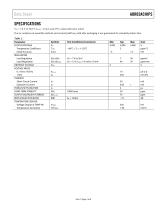
Data Sheet SPECIFICATIONS VIN = 7.0 V to 36.0 V, ILOAD = 0 mA, and 25°C, unless otherwise noted. Due to variations in assembly methods and normal yield loss, yield after packaging is not guaranteed for standard product dice. Table 2. Parameter OUTPUT VOLTAGE Temperature Coefficient Initial Accuracy REGULATION Line Regulation Load Regulation DROPOUT VOLTAGE VOLTAGE NOISE 0.1 Hz to 10.0 Hz 1 kHz CURRENT Short-Circuit Current Quiescent Current TURN-IN SETTLING TIME LONG-TERM STABILITY OUTPUT VOLTAGE HYSTERESIS RIPPLE REJECTION RATIO TEMPERATURE SENSOR Voltage Output at TEMP Pin Temperature Sensitivity...
Open the catalog to page 3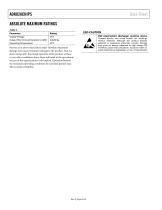
Data Sheet ABSOLUTE MAXIMUM RATINGS Stresses at or above those listed under Absolute Maximum Ratings may cause permanent damage to the product. This is a stress rating only; functional operation of the product at these or any other conditions above those indicated in the operational section of this specification is not implied. Operation beyond the maximum operating conditions for extended periods may affect product reliability. ESD (electrostatic discharge) sensitive device. Charged devices and circuit boards can discharge without detection. Although this product features patented or proprietary...
Open the catalog to page 4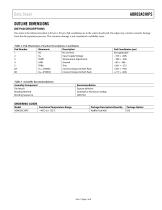
Data Sheet OUTLINE DIMENSIONS DIE PAD DESCRIPTIONS Die center is the reference location at 0.0 µm × 0.0 µm. Pad coordinates are to the center of each pad. Die edges may contain cosmetic damage from the die separation process. This cosmetic damage is not considered a reliability issue. Table 4. Pad Mnemonics, Function Descriptions, Coordinates Pad Number 1 2 3 4 5 6A 6B Mnemonic NC VIN TEMP GND TRIM VOUT (SENSE) VOUT (FORCE) Description No Connect Input Supply Voltage Temperature Adjustment Ground Trim Connect Output to Both Pads Connect Output to Both Pads Table 5. Assembly Recommendations Assembly...
Open the catalog to page 5
Data Sheet
Open the catalog to page 6
Data Sheet
Open the catalog to page 7
Data Sheet ©2014 Analog Devices, Inc. All rights reserved. Trademarks and registered trademarks are the property of their respective owners. D12376-0-5/14(0)
Open the catalog to page 8All Analog Devices catalogs and technical brochures
 HMC722LP3E
8 Pages
 Isolated Sigma-Delta Modulator
17 Pages
 HMC853 Data Sheet
10 Pages
 AN-1084
8 Pages
 AN-1091
2 Pages
 AN_737
8 Pages
 AN-0982
4 Pages
 ADF7024
24 Pages
 AD9915
48 Pages
 AD9914
48 Pages
 ADRF6612
59 Pages
 ADRF6820
48 Pages
 ADL5246
32 Pages
 ADA4961
22 Pages
 AN-1141
8 Pages
 AN-698
36 Pages
 Temperature Sensors
2 Pages
 Reference Circuits
8 Pages
 Precision ADCs
16 Pages
 AD9364 RF Agile Transceiver
32 Pages
 Digital Temperature Sensors
2 Pages
 Digital to Analog Converter ICs
12 Pages
 AD1836A: Multichannel 96 kHz Codec
24 Pages


Archived catalogs
 Zero-Drift Amplifiers
2 Pages
 Powering ADI Components
8 Pages


- Ethernet switch
- Industrial network switch
- Acceleration sensor
- Unmanaged switch
- Transceiver module
- Analog Devices motor controller
- Triaxial acceleration sensor
- DC motor controller
- Data acquisition unit
- Analog Devices stepper motor controller
- Industrial converter
- Ethernet transceiver
- Processor
- High-voltage amplifier
- Low-noise amplifier
- Multiplexer
- Compact motor controller
- Gyroscope
- Closed-loop motor controller
- Digital converter