- Catalogs
- Analog Devices
- ADP5133: Dual 3 MHz, 800 mA Buck Regulators in WLCSP
ADP5133: Dual 3 MHz, 800 mA Buck Regulators in WLCSP
1 /24Pages

ADP5133: Dual 3 MHz, 800 mA Buck Regulators in WLCSP
1 /24Pages
Catalog excerpts
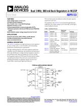
Dual 3 MHz, 800 mA Buck Regulators in WLCSP Data Sheet FEATURES The two bucks operate out of phase to reduce the input capacitor requirement and noise. Input voltage range: 2.3 V to 5.5 V Two 800 mA buck regulators Tiny, 16-ball, 2 mm × 2 mm WLCSP package Regulator accuracy: ±1.8% Factory programmable or external adjustable VOUTx 3 MHz buck operation with forced PWM and auto PWM/PSM modes BUCK1/BUCK2: output voltage range from 0.8 V to 3.8 V The regulators in the ADP5133 are activated through dedicated enable pins. The output voltages can be externally set through a resistor feedback network. Table 1. Related Devices Maximum Current 800 mA, 300 mA 1.2 A, 300 mA 1.2 A, 300 mA APPLICATIONS Power for processors, ASICs, FPGAs, and RF chipsets Portable instrumentation and medical devices Space constrained devices GENERAL DESCRIPTION Channels 2 Bucks, 1 LDO 2 Bucks, 1 LDO 2 Bucks, 2 LDOs 2 Bucks, 2 LDOs 2 Bucks, 2 LDOs with 2 ENx pins 1 Buck, 2 LDOs 1 Buck, 2 LDOs with supervisory, watchdog, manual reset 2 Bucks with 2 ENx pins 2 Bucks, 2 LDOs with precision enable and power-good output The ADP5133 combines two high performance buck regulators in a tiny, 16-ball, 2 mm × 2 mm WLCSP to meet demanding performance and board space requirements. The high switching frequency of the buck regulators enables tiny multilayer external components and minimizes the board space. When the MODE pin is set high, the buck regulators operate in forced PWM mode. When the MODE pin is set low and the buck regulators operate in PWM mode, the load current is above a predefined threshold. When the load current falls below a predefined threshold, the regulators operate in power save mode (PSM), improving the light load efficiency. Package LFCSP (CP-24-10) LFCSP (CP-24-10) LFCSP (CP-24-10), TSSOP (RE-28-1) LFCSP (CP-24-10) WLCSP (CB-16-8) TYPICAL APPLICATION CIRCUIT ADP5133 VOUT1 2.3V TO 5.5V FPWM AUTO Document Feedback Information furnished by Analog Devices is believed to be accurate and reliable. However, no responsibility is assumed by Analog Devices for its use, nor for any infringements of patents or other rights of third parties that may result from its use. Specifications subject to change without notice. No license is granted by implication or otherwise under any patent or patent rights of Analog Devices. Trademarks and registered trademarks are the property of their respective owners. One Technology Way, P.O. Box 9106, Norwood, MA 02062-9106, U.S.A. Tel: 781.329.4700 ©2014 Analog Devices, Inc. All rights reserved. Technical Support www.analog.com
Open the catalog to page 1
Data Sheet REVISION HISTORY 4/14—Revision 0: Initial Version
Open the catalog to page 2
Data Sheet SPECIFICATIONS GENERAL SPECIFICATIONS VIN1 = VIN2 = 2.3 V to 5.5 V, TJ = −40°C to +125°C for minimum/maximum specifications, and TA = 25°C for typical specifications, unless otherwise noted. Table 2. Parameter INPUT VOLTAGE RANGE THERMAL SHUTDOWN Threshold Hysteresis START-UP TIME1 BUCK1 BUCK2 EN1, EN2, MODE INPUTS Input Logic High Input Logic Low Input Leakage Current STANDBY CURRENT All Channels Enabled All Channels Disabled VIN1 UNDERVOLTAGE LOCKOUT UVLO Input Voltage Rising UVLO Input Voltage Falling 1 Test Conditions/Comments TSSD TSSD-HYS ISTBY-NOSW ISHUTDOWN Start-up time is...
Open the catalog to page 3
Data Sheet BUCK1 AND BUCK2 SPECIFICATIONS VIN1 = VIN2 = 2.3 V to 5.5 V; TJ = −40°C to +125°C for minimum/maximum specifications, and TA = 25°C for typical specifications, unless otherwise noted. All limits at temperature extremes are guaranteed via correlation using standard statistical quality control (SQC). Table 3. Parameter INPUT CHARACTERISTICS Input Voltage Range OUTPUT CHARACTERISTICS Output Voltage Accuracy Line Regulation Load Regulation VOLTAGE FEEDBACK PSM CURRENT THRESHOLD PSM to PWM Operation OPERATING SUPPLY CURRENT BUCK1 Only Test Conditions/Comments BUCK2 Only BUCK1 and BUCK2...
Open the catalog to page 4
Data Sheet ABSOLUTE MAXIMUM RATINGS Storage Temperature Range Operating Junction Temperature Range Soldering Conditions Stresses at or above those listed under Absolute Maximum Ratings may cause permanent damage to the product. This is a stress rating only; functional operation of the product at these or any other conditions above those indicated in the operational section of this specification is not implied. Operation beyond the maximum operating conditions for extended periods may affect product reliability. For detailed information on power dissipation, see the Power Dissipation and Thermal...
Open the catalog to page 5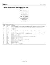
Data Sheet PIN CONFIGURATION AND FUNCTION DESCRIPTIONS BALL A1 INDICATOR 2 AGND AGND TOP VIEW (BALL SIDE DOWN) Not to Scale Table 7. Pin Function Descriptions Pin No. A1 AGND MODE Description BUCK1 Feedback Input. For device models with an adjustable output voltage, connect this pin to the middle of the BUCK1 resistor divider. For device models with a fixed output voltage, leave this pin unconnected. Analog Ground. Analog Ground. BUCK2 Feedback Input. For device models with an adjustable output voltage, connect this pin to the middle of the BUCK2 resistor divider. For device models with a fixed...
Open the catalog to page 6
Data Sheet TYPICAL PERFORMANCE CHARACTERISTICS VIN1 = VIN2 = 3.6 V, TA = 25°C, unless otherwise noted. 140 3.310 Figure 3. System Quiescent Current vs. Input Voltage, VOUT1 = 1.8 V, VOUT2 = 1.8 V, All Channels Enabled Figure 6. BUCK1 Load Regulation Across Temperature, VIN = 4.2 V, VOUT1 = 3.3 V, PWM Mode 1.812 Figure 7. BUCK2 Load Regulation Across Temperature,VIN = 3.6 V, VOUT2 = 1.8 V, PWM Mode Figure 8. BUCK1 Load Regulation Across Temperature, VIN = 3.6 V, VOUT1 = 0.8 V, PWM Mode
Open the catalog to page 7
Figure 9. BUCK1 Efficiency vs. Load Current, Across Input Voltage, VOUT1 = 3.3 V, Auto PWM/PSM Mode Figure 10. BUCK1 Efficiency vs. Load Current, Across Input Voltage, VOUT1 = 3.3 V, PWM Mode Figure 13. BUCK1 Efficiency vs. Load Current, Across Input Voltage, VOUT1 = 0.8 V, Auto PWM/PSM Mode Figure 11. BUCK2 Efficiency vs. Load Current, Across Input Voltage, VOUT2 = 1.8 V, Auto PWM/PSM Mode Figure 12. BUCK2 Efficiency vs. Load Current, Across Input Voltage, VOUT2 = 1.8 V, PWM Mode Figure 14. BUCK1 Efficiency vs. Load Current, Across Input Voltage, VOUT1 = 0.8 V, PWM Mode
Open the catalog to page 8All Analog Devices catalogs and technical brochures
 HMC722LP3E
8 Pages
 Isolated Sigma-Delta Modulator
17 Pages
 HMC853 Data Sheet
10 Pages
 AN-1084
8 Pages
 AN-1091
2 Pages
 AN_737
8 Pages
 AN-0982
4 Pages
 ADF7024
24 Pages
 AD9915
48 Pages
 AD9914
48 Pages
 ADRF6612
59 Pages
 ADRF6820
48 Pages
 ADL5246
32 Pages
 ADA4961
22 Pages
 AN-1141
8 Pages
 AN-698
36 Pages
 Temperature Sensors
2 Pages
 Reference Circuits
8 Pages
 Precision ADCs
16 Pages
 ADR02ACHIPS: ADR02ACHIPS
8 Pages
 AD9364 RF Agile Transceiver
32 Pages
 Digital Temperature Sensors
2 Pages
 Digital to Analog Converter ICs
12 Pages
 AD1836A: Multichannel 96 kHz Codec
24 Pages


Archived catalogs
 Zero-Drift Amplifiers
2 Pages
 Powering ADI Components
8 Pages


- Ethernet switch
- Industrial network switch
- Acceleration sensor
- Unmanaged switch
- Transceiver module
- Analog Devices motor controller
- Triaxial acceleration sensor
- DC motor controller
- Data acquisition unit
- Analog Devices stepper motor controller
- Industrial converter
- Ethernet transceiver
- High-voltage amplifier
- Low-noise amplifier
- Multiplexer
- Compact motor controller
- Gyroscope
- Closed-loop motor controller
- Digital converter