- Catalogs
- Analog Devices
- ADP5080: High Efficiency Integrated Power Solution for Multicell Lithium Ion Applications
ADP5080: High Efficiency Integrated Power Solution for Multicell Lithium Ion Applications
1 /64Pages

ADP5080: High Efficiency Integrated Power Solution for Multicell Lithium Ion Applications
1 /64Pages
Catalog excerpts

FUNCTIONAL BLOCK DIAGRAM Wide input voltage range: 4.0 V to 15 V High efficiency architecture Up to 2 MHz switching frequency 6 synchronous rectification dc-to-dc converters Channel 1 buck regulator: 3 A maximum Channel 2 buck regulator: 1.15 A maximum Channel 3 buck regulator: 1.5 A maximum Channel 4 buck regulator: 0.8 A maximum Channel 5 buck regulator: 2 A maximum Channel 6 configurable buck or buck boost regulator 2 A maximum for buck regulator configuration 1.5 A maximum for buck boost regulator configuration Channel 7 high voltage, high performance LDO regulator: 30 mA maximum 2 low quiescent current keep-alive LDO regulators LDO1 regulator: 400 mA maximum LDO2 regulator: 300 mA maximum Control circuit Charge pump for internal switching driver power supply I2C-programmable output levels and power sequencing Package: 72-ball, 4.5 mm × 4.0 mm × 0.6 mm WLCSP (0.5 mm pitch) CONTROL LOGIC VOLTAGE REFERENCE FAULT CHARGE PUMP 4V TO 15V CH 6 BUCK BOOST REGULATOR Data Sheet High Efficiency Integrated Power Solution for Multicell Lithium Ion Applications ADP5080 APPLICATIONS DSLR cameras Non-reflex (mirrorless) cameras Portable instrumentation GENERAL DESCRIPTION The ADP5080 is a fully integrated, high efficiency power solution for multicell lithium ion battery applications. The device can connect directly to the battery, which eliminates the need for preregulators and, therefore, increases the battery life of the system. The ADP5080 integrates two keep-alive LDO regulators, five synchronous buck regulators, a configurable four-switch buck boost regulator, and a high voltage LDO regulator. The ADP5080 is a highly integrated power solution that incorporates all power MOSFETs, feedback loop compensation, voltage setting resistor dividers, and discharge switches, as well as a charge pump to generate a global bootstrap voltage. All these features help to minimize the number of external components and PCB space required, providing significant advantages for portable applications. The switching frequency is selectable on each channel from 750 kHz to 2 MHz. Key functions for power applications, such as soft start, selectable preset output voltage, and flexible power-up and power-down sequences, are provided on chip and are programmable via the I2C interface with fused factory defaults. The ADP5080 is available in a 72-ball WLCSP 0.5 mm pitch package. Document Feedback Information furnished by Analog Devices is believed to be accurate and reliable. However, no responsibility is assumed by Analog Devices for its use, nor for any infringements of patents or other rights of third parties that may result from its use. Specifications subject to change without notice. No license is granted by implication or otherwise under any patent or patent rights of Analog Devices. Trademarks and registered trademarks are the property of their respective owners. One Technology Way, P.O. Box 9106, Norwood, MA 02062-9106, U.S.A. Tel: 781.329.4700 ©2013–2014 Analog Devices, Inc. All rights reserved. Technical Support www.analog.com
Open the catalog to page 1
Data Sheet REVISION HISTORY 4/14—Revision A: Initial Version
Open the catalog to page 2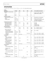
Data Sheet SPECIFICATIONS TJ = 25°C, VVBATT = 7.2 V, VVREG1 = VVDRx = 5 V, VVREG2 = VVDDIO = 3.3 V, unless otherwise noted. Table 1. Parameter INPUT SUPPLY VOLTAGE RANGE VBATT VILDO7 VDDIO QUIESCENT CURRENT Operating Quiescent Current VDDIO Standby Current UNDERVOLTAGE LOCKOUT UVLO Rising Threshold UVLO Falling Threshold VBATT UVLO Threshold Reset Threshold OSCILLATOR CIRCUIT Switching Frequency UVLO VUVLO (R) VUVLO (F) VUVLO (BATT) VUVLO (POR) SYNC Pin, Input Clock Frequency Range Minimum On Pulse Width Minimum Off Pulse Width High Logic Low Logic LOGIC INPUTS EN Pin High Level Threshold Low...
Open the catalog to page 3
ADP5080 Parameter POWER GOOD Rising Threshold Falling Threshold OVERVOLTAGE/UNDERVOLTAGE OVP Threshold UVP Threshold THERMAL SHUTDOWN Rising Threshold Hysteresis Data Sheet Symbol VPGOOD (R) VPGOOD (F) VOVP VUVP TSD TTSD TTSD_HYS Test Conditions/Comments Measured at VOUT Measured at VOUT Measured at VOUT Measured at VOUT HOUSEKEEPING BLOCK SPECIFICATIONS TJ = 25°C, VVBATT = 7.2 V, VVREG1 = VVDRx = 5 V, VVREG2 = VVDDIO = 3.3 V, unless otherwise noted. Table 2. Parameter LDO1 Output Voltage (VREG1 Pin) Fixed Voltage Range, 1 Bit Voltage Accuracy Load Regulation Line Regulation Current-Limit Threshold...
Open the catalog to page 4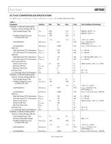
Data Sheet DC-TO-DC CONVERTER BLOCK SPECIFICATIONS TJ = 25°C, VVBATT = 7.2 V, VVREG1 = VVDRx = 5 V, VVREG2 = VVDDIO = 3.3 V, unless otherwise noted. Table 3. Parameter CHANNEL 1 SYNC BUCK REGULATOR Channel 1 Output Voltage (FB1 Pin) Fixed Voltage Range, 5 Bits Test Conditions/Comments Feedback Voltage Accuracy at Default VID Code Load Regulation Line Regulation SW1A Pin High-Side Power FET On Resistance Low-Side Power FET On Resistance SW1B Pin High-Side Power FET On Resistance Low-Side Power FET On Resistance SW1A and SW1B Pins Switch Current Limit Minimum Off Time Minimum Duty Cycle Soft Start...
Open the catalog to page 5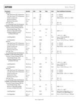
ADP5080 Parameter SW3 Pins High-Side Power FET On Resistance Low-Side Power FET On Resistance Switch Current Limit Minimum Off Time Minimum Duty Cycle Soft Start Time COUT Discharge Switch On Resistance CHANNEL 4 SYNC BUCK REGULATOR Channel 4 Output Voltage (FB4 Pin) Fixed Voltage Range, 3 Bits Minimum Adjustable Voltage Feedback Voltage Accuracy at Default VID Code Line Regulation SW4 Pin High-Side Power FET On Resistance Low-Side Power FET On Resistance Switch Current Limit Minimum On Time Maximum Duty Cycle Soft Start Time COUT Discharge Switch On Resistance CHANNEL 5 SYNC BUCK REGULATOR Channel...
Open the catalog to page 6
Data Sheet Parameter SW6A Pins Low-Side Power FET On Resistance High-Side Power FET On Resistance High-Side Switch Current Limit Minimum On Time SW6B Pins Low-Side Power FET On Resistance High-Side Power FET On Resistance Boost Minimum Duty Cycle Soft Start Time COUT Discharge Switch On Resistance Test Conditions/Comments ID = 100 mA, VVDR6 = 5 V ID = 100 mA, VVDR6 = 5 V Peak current, −25°C ≤ TJ ≤ +85°C SW6A high-side on time ID = 100 mA ID = 100 mA SW6B low-side duty cycle SS6 = 10 VVOUT6 = 1 V LINEAR REGULATOR BLOCK SPECIFICATIONS TJ = 25°C, VVBATT = 7.2 V, VVREG1 = VVDRx = 5 V, VVREG2 = VVDDIO...
Open the catalog to page 7All Analog Devices catalogs and technical brochures
 HMC722LP3E
8 Pages
 Isolated Sigma-Delta Modulator
17 Pages
 HMC853 Data Sheet
10 Pages
 AN-1084
8 Pages
 AN-1091
2 Pages
 AN_737
8 Pages
 AN-0982
4 Pages
 ADF7024
24 Pages
 AD9915
48 Pages
 AD9914
48 Pages
 ADRF6612
59 Pages
 ADRF6820
48 Pages
 ADL5246
32 Pages
 ADA4961
22 Pages
 AN-1141
8 Pages
 AN-698
36 Pages
 Temperature Sensors
2 Pages
 Reference Circuits
8 Pages
 Precision ADCs
16 Pages
 ADR02ACHIPS: ADR02ACHIPS
8 Pages
 AD9364 RF Agile Transceiver
32 Pages
 Digital Temperature Sensors
2 Pages
 Digital to Analog Converter ICs
12 Pages
 AD1836A: Multichannel 96 kHz Codec
24 Pages


Archived catalogs
 Zero-Drift Amplifiers
2 Pages
 Powering ADI Components
8 Pages


- Ethernet switch
- Industrial network switch
- Acceleration sensor
- Unmanaged switch
- Transceiver module
- Analog Devices motor controller
- Triaxial acceleration sensor
- DC motor controller
- Data acquisition unit
- Analog Devices stepper motor controller
- Industrial converter
- Ethernet transceiver
- Processor
- High-voltage amplifier
- Low-noise amplifier
- Multiplexer
- Compact motor controller
- Gyroscope
- Closed-loop motor controller
- Digital converter