
- Catalogs
- Analog Devices
- ADP2311:Dual 1 A, 18 V, Synchronous Step-Down Regulator with Fail-Safe Voltage Monitoring


- Products
- Catalogs
- News & Trends
- Exhibitions
ADP2311:Dual 1 A, 18 V, Synchronous Step-Down Regulator with Fail-Safe Voltage Monitoring
ADP2311:Dual 1 A, 18 V, Synchronous Step-Down Regulator with Fail-Safe Voltage Monitoring
- Input voltage range: 4.5 V to 18 V
- ±1.0% output accuracy
- Integrated MOSFETs with typical resistances of 110 mΩ (high-side) and 60 mΩ (low-side)
- Continuous output current: 1 A per channel
- Power fail comparator and power-on reset with programmable delay
- Adjustable voltage monitor for power-down
- Watchdog timer for system reliability
- 180° out-of-phase operation to reduce input ripple
- Fixed switching frequency of 300 kHz
- Protection features: UVLO, OCP, OVP, and thermal shutdown
- Power input voltage range: 4.5 V to 18 V
- Quiescent current: 1.2 mA typical
- Shutdown current: 10 µA typical
- Feedback regulation voltage: 0.6 V
- Internal regulator voltage: 5 V
- Switching frequency: 300 kHz
- Thermal shutdown threshold: 150°C
- Input Capacitor Selection: Use a ceramic capacitor (10 μF to 47 μF) close to the PVINx pin. Ensure the voltage rating exceeds the maximum input voltage.
- Output Voltage Setting: Set using an external resistor divider. Ensure RBOT is less than 30 kΩ to maintain accuracy.
- Inductor Selection: Choose based on operating frequency, input/output voltage, and ripple current. The inductor value affects transient response and efficiency.
- Output Capacitor Selection: Use small ceramic capacitors with low ESR and ESL. X5R or X7R dielectrics are recommended.
Catalog excerpts

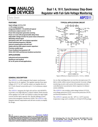
Dual 1 A, 18 V, Synchronous Step-Down Regulator with Fail-Safe Voltage Monitoring Data Sheet TYPICAL APPLICATION CIRCUIT Input voltage: 4.5 V to 18 V ±1.0% output accuracy Integrated MOSFET: 110 mΩ/60 mΩ typical Continuous output current: 1 A/1 A Power fail comparator generates warning Power-on reset with programmable delay timer Adjustable voltage monitor for power-down (Channel 2) Watchdog refresh input Dual phase with 180° out-of-phase operation Fixed switching frequency: 300 kHz Internal compensation and soft start Stable with low ESR output ceramic capacitors Precision enable input Power feedback during power-off UVLO, OCP, OVP, and thermal shutdown protection Figure 1. 100 VOUT = 3.3V VOUT = 5V APPLICATIONS EFFICIENCY (%) Industrial and instrumentation Healthcare and medical DC-to-DC point of load applications Figure 2. Efficiency vs. Output Current at VIN = 12 V, fSW = 300 kHz GENERAL DESCRIPTION The ADP2311 is a fully integrated, dual output, synchronous step-down dc-to-dc regulator. The regulator operates from input voltages of 4.5 V to 18 V, and the output can regulate down to 0.6 V. Each channel can provide up to 1 A of continuous output current. An on-chip watchdog timer can reset the microprocessor if it fails to strobe within a preset timeout period. Accurate voltage monitoring circuitry and a power fail comparator provide a controlled power-up and power-down sequence to enhance system reliability. The ADP2311 integrates the high-side and low-side MOSFETs to provide a very high efficiency, compact solution. Both channels of the regulator run at 180° out of phase to reduce the input ripple current and the input capacitor size, thereby helping to lower system electromagnetic interference (EMI). The ADP2311 also integrates internal compensation and soft start circuitry to simplify the design. The ADP2311 also includes undervoltage lockout (UVLO), overvoltage protection (OVP), overcurrent protection (OCP), and thermal shutdown (TSD). The ADP2311 operates over the −40°C to +125°C junction temperature range and is available in a 24-lead LFCSP package. Document Feedback Information furnished by Analog Devices is believed to be accurate and reliable. However, no responsibility is assumed by Analog Devices for its use, nor for any infringements of patents or other rights of third parties that may result from its use. Specifications subject to change without notice. No license is granted by implication or otherwise under any patent or patent rights of Analog Devices. Trademarks and registered trademarks are the property of their respective owners. One Technology Way, P.O. Box 9106, Norwood, MA 02062-9106, U.S.A. Tel: 781.329.4700 ©2014 Analog Devices, Inc. All rights reserved. Technical Support www.analog.com
Open the catalog to page 1
Data Sheet REVISION HISTORY 3/14—Revision A: Initial Version
Open the catalog to page 2
Data Sheet FUNCTIONAL BLOCK DIAGRAM UVLO BOOST REGULATOR I1MAX SLOPE RAMP1 SOFT START CONTROL LOGIC AND MOSFET DRIVER WITH ANTI-CROSS PROTECTION VREG DRIVER PGND1 LOW-SIDE CURRENT – SENSE TIMER POR DELAY TIMER POWER-UP AND POWER-DOWN SEQUENCE CONTROL RSTO RESET GENERATOR HICCUP MODE BOOST REGULATOR CONTROL LOGIC AND MOSFET DRIVER WITH ANTI-CROSS PROTECTION VREG DRIVER PGND2 LOW-SIDE CURRENT SENSE + SOFT START
Open the catalog to page 3
Data Sheet SPECIFICATIONS PVIN1 = PVIN2 = 12 V, TJ = −40°C to +125°C, unless otherwise noted. Table 1. Parameter POWER INPUT Power Input Voltage Range Quiescent Current (PVIN1 + PVIN2) Shutdown Current (PVIN1 + PVIN2) PVINx Undervoltage Lockout Threshold PVINx Rising PVINx Falling FEEDBACK FBx Regulation Voltage FBx Bias Current INTERNAL REGULATOR VREG Voltage Dropout Voltage Regulator Current Limit MOSFET ON RESISTANCE High-Side On Resistance Low-Side On Resistance CURRENT LIMIT High-Side Peak Current Limit Low-Side Source Current Limit Low-Side Sink Current Limit Hiccup Time SWITCH NODE SWx...
Open the catalog to page 4
Data Sheet Parameter VOLTAGE MONITOR COMPARATOR VM2 Input Threshold VM2 Input Hysteresis VM2 Leakage Current POR TIMER TIMER Pin Pull-Up Current WATCHDOG Reset Threshold Voltage Reset Threshold Hysteresis Reset Timeout Period Watchdog Timeout Period Option 1 Option 2 Option 3 Option 4 WDI Pulse Width WDI Input High Voltage WDI Input Low Voltage RSTO Output Low Voltage RSTO Leakage Current Test Conditions/Comments VM2 pin Falling threshold TIMER pin 3 WDI and RSTO pins Senses VFB2 tRP tWD THERMAL Thermal Shutdown Threshold Thermal Shutdown Hysteresis
Open the catalog to page 5
Data Sheet ABSOLUTE MAXIMUM RATINGS PGNDx toGND Operating Temperature Range Storage Temperature Range Soldering Conditions Stresses above those listed under Absolute Maximum Ratings may cause permanent damage to the device. This is a stress rating only; functional operation of the device at these or any other conditions above those indicated in the operational section of this specification is not implied. Exposure to absolute maximum rating conditions for extended periods may affect device reliability. THERMAL RESISTANCE 6JA is specified for the worst-case conditions, that is, a device soldered...
Open the catalog to page 6
Data Sheet PIN CONFIGURATION AND FUNCTION DESCRIPTIONS NOTES 1. SOLDER THE EXPOSED PAD TO AN EXTERNAL GND PLANE. Table 4. Pin Function Descriptions Pin No. 1 2 Description Analog Ground. Connect this pin to the ground plane. Internal 5 V Regulator Output. The IC control circuits are powered from this voltage. Place a 1 µF ceramic capacitor between VREG and GND. POR Sequence Selection and Delay Time Setting. This pin is used to set the POR sequence and delay time (see the TIMER Pin Configuration section). Power Fail Comparator Input. Connect an external resistor divider from PVIN2 to PFI to monitor...
Open the catalog to page 7
Data Sheet TYPICAL PERFORMANCE CHARACTERISTICS TA = 25°C, VIN = 12 V, VOUT = 3.3 V, L = 22 µH, COUT = 47 µF/X7R/6.3 V, fSW = 300 kHz, unless otherwise noted. 95 VOUT = 1V VOUT = 1.2V VOUT = 1.5V VOUT = 1.8V VOUT = 2.5V VOUT = 3.3V VOUT = 5V Figure 8. Efficiency vs. Output Current at VIN = 5 V Figure 5. Efficiency vs. Output Current at VIN = 12 V VOUT = 1V VOUT = 1.2V VOUT = 1.5V VOUT = 1.8V VOUT = 2.5V VOUT = 3.3V Figure 6. Shutdown Current vs. VIN Figure 9. Quiescent Current vs. VIN Figure 7. UVLO Threshold vs. Temperature Figure 10. Enable Threshold vs. Temperature
Open the catalog to page 8All Analog Devices catalogs and technical brochures
 HMC722LP3E
8 Pages
 Isolated Sigma-Delta Modulator
17 Pages
 HMC853 Data Sheet
10 Pages
 AN-1084
8 Pages
 AN-1091
2 Pages
 AN_737
8 Pages
 AN-0982
4 Pages
 ADF7024
24 Pages
 AD9915
48 Pages
 AD9914
48 Pages
 ADRF6612
59 Pages
 ADRF6820
48 Pages
 ADL5246
32 Pages
 ADA4961
22 Pages
 AN-1141
8 Pages
 AN-698
36 Pages
 Temperature Sensors
2 Pages
 Reference Circuits
8 Pages
 Precision ADCs
16 Pages
 ADR02ACHIPS: ADR02ACHIPS
8 Pages
 AD9364 RF Agile Transceiver
32 Pages
 Digital Temperature Sensors
2 Pages
 Digital to Analog Converter ICs
12 Pages
 AD1836A: Multichannel 96 kHz Codec
24 Pages



























Archived catalogs
 Zero-Drift Amplifiers
2 Pages
 Powering ADI Components
8 Pages




- Ethernet switch
- Industrial network switch
- Acceleration sensor
- Unmanaged switch
- Analog Devices motor controller
- Transceiver module
- Triaxial acceleration sensor
- DC motor controller
- Data acquisition unit
- Analog Devices stepper motor controller
- Industrial converter
- Ethernet transceiver
- High-voltage amplifier
- Low-noise amplifier
- Multiplexer
- Compact motor controller
- Digital converter
- Closed-loop motor controller
- Digital motor controller