ADP2165/ADP2166: 5.5 V, 5A/6A, High Efficiency, Step-Down DC-to-DC Regulators with Output Tracking Data Sheet
1 /
23Pages
Catalog excerpts
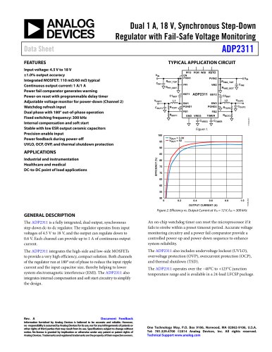
TYPICAL APPLICATION CIRCUIT Continuous output current ADP2165: 5 A ADP2166: 6 A Integrated MOSFET High-side on resistance: 19 mΩ Low-side on resistance: 15 mΩ Reference voltage: 0.6 V ± 1% over temperature range Input voltage range: 2.7 V to 5.5 V Current mode architecture Switching frequency Fixed frequency: 620 kHz or 1.2 MHz Adjustable frequency: 250 kHz to 1.4 MHz Synchronizes to external clock: 250 kHz to 1.4 MHz Selectable synchronize phase shift: in phase or out of phase External compensation Programmable soft start Startup into a precharged output Voltage tracking input Power-good output and precision enable input Accurate current limit Available in 24-lead, 4 mm × 4 mm LFCSP_WQ package Supported by ADIsimPower™ design tool APPLICATIONS Point of load regulation Communications and networking High end consumer Industrial, instrumentation, and healthcare The ADP2165/ADP2166 are designed to be extremely flexible with the addition of a minimal amount of external components to program soft start and control loop compensation. The ADP2165/ADP2166 are supplied from an input voltage of 2.7 V to 5.5 V. Output voltage options include 3.3 V, 2.5 V, 1.8 V, 1.5 V, 1.2 V, or 1.0 V fixed outputs and adjustable options capable of supporting an output voltage range from 0.6 V to 90% of the input voltage. Protection features include undervoltage lockout (UVLO), overvoltage protection (OVP), overcurrent protection (OCP), and thermal shutdown (TSD) for robust performance. The ADP2165/ADP2166 operate over the −40°C to +125°C junction temperature range and are available in a 24-lead LFCSP_WQ package. GENERAL DESCRIPTION Key features include precision enable, power-good monitor, and output voltage tracking to facilitate robust sequencing. The switching frequency can be programmed from 250 kHz to 1.4 MHz, or it can be fixed at 620 kHz or 1.2 MHz. The synchronization function allows the switching frequency to synchronize to an external clock, minimizing the electromagnetic interference (EMI) of the system. VPVIN = 3.3V 95 90 VPVIN = 5V 85 EFFICIENCY (%) The ADP2165/ADP2166 are high efficiency, current mode control, step-down dc-to-dc regulators with an integrated 19 mΩ high-side FET and a 15 mΩ synchronous rectified FET. The ADP2165/ADP2166 combine a small size, 4 mm × 4 mm LFCSP package with an accurate current limit, resulting in a smaller inductor size and a high power density, point of load solution. Data Sheet 5.5 V, 5 A/6 A, High Efficiency, Step-Down DC-to-DC Regulators with Output Tracking ADP2165/ADP2166 Figure 2. Efficiency vs. Output Current Document Feedback Information furnished by Analog Devices is believed to be accurate and reliable. However, no responsibility is assumed by Analog Devices for its use, nor for any infringements of patents or other rights of third parties that may result from its use. Specifications subject to change without notice. No license is granted by implication or otherwise under any patent or patent rights of Analog Devices. Trademarks and registered trademarks are the property of their respective owners. One Technology Way, P.O. Box 9106, Norwood, MA 02062-9106, U.S.A. Tel: 781.329.4700 ©2014 Analog Devices, Inc. All rights reserved. Technical Support www.analog.com
Open the catalog to page 1Data Sheet REVISION HISTORY 8/14—Revision 0: Initial Version
Open the catalog to page 2Data Sheet FUNCTIONAL BLOCK DIAGRAM EN SLOPE RAMP HICCUP MODE VPVIN CONTROL LOGIC PGOOD AVIN SLOPE RAMP Figure 3. ADP2165/ADP2166 Functional Block Diagram
Open the catalog to page 3Data Sheet SPECIFICATIONS VPVIN = VAVIN = 5 V, TJ = −40°C to +125°C for minimum/maximum specifications, and TA = 25°C for typical specifications, unless otherwise noted. Table 1. Parameter PVIN AND AVIN VPVIN Voltage Range VAVIN Voltage Range Quiescent Current Shutdown Current VAVIN Undervoltage Lockout Threshold FB FB Regulation Voltage Fixed Output Version FB Bias Current ERROR AMPLIFIER (EA) Transconductance EA Source Current EA Sink Current INTERNAL REGULATOR (VREG) VREG Voltage Dropout Voltage Regulator Current Limit SW High-Side On Resistance 1 Symbol VPVIN VAVIN IQ ISHDN UVLO No...
Open the catalog to page 4' Pin-to-pin measurement.
Open the catalog to page 5Data Sheet ABSOLUTE MAXIMUM RATINGS SS, COMRTRK, VREG, SYNC, RT Operating Junction Temperature Range Storage Temperature Range Soldering Conditions Stresses at or above those listed under Absolute Maximum Ratings may cause permanent damage to the product. This is a stress rating only; functional operation of the product at these or any other conditions above those indicated in the operational section of this specification is not implied. Operation beyond the maximum operating conditions for extended periods may affect product reliability. THERMAL RESISTANCE 6JA is specified for the...
Open the catalog to page 6Data Sheet PIN CONFIGURATION AND FUNCTION DESCRIPTIONS NOTES 1. EXPOSED PAD. SOLDER THE EXPOSED PAD TO AN EXTERNAL GROUND PLANE UNDERNEATH THE IC FOR THERMAL DISSIPATION. Table 4. Pin Function Descriptions Pin No. 1 Mnemonic SYNC SS COMP FB GND PGOOD BST PGND Description Synchronization Input. Connect this pin to an external clock between 250 kHz and 1.4 MHz to synchronize the switching frequency to the external clock. RT can be used to program the phase shift when synchronizing the external clock. Frequency Setting. Connect a resistor between the RT and GND pins to program the switching...
Open the catalog to page 7Data Sheet TYPICAL PERFORMANCE CHARACTERISTICS TA = 25°C, VPVIN = VAVIN = 5 V, VOUT = 1.2 V, L = 1 µH, CIN = 47 µF, COUT = 100 µF, fSW = 600 kHz, unless otherwise noted. 100 Figure 5. Efficiency (fSW = 600 kHz, VPVIN = 3.3 V) vs. Output Current INDUCTOR: WÜRTH ELEKTRONIK 744311100 INDUCTOR: WÜRTH ELEKTRONIK 744311100 Figure 8. Efficiency (fSW = 600 kHz, VPVIN = 5 V) vs. Output Current 55 INDUCTOR: WÜRTH ELEKTRONIK 744314047 INDUCTOR: WÜRTH ELEKTRONIK 744314047 0 Figure 6. Efficiency (fSW = 1.2 MHz, VPVIN = 3.3 V) vs. Output Current Figure 9. Efficiency (fSW = 1.2 MHz, VPVIN = 5 V) vs....
Open the catalog to page 8Data Sheet Figure 11. High-Side NFET Resistor vs. VPVIN (Pin-to-Pin Measurements) Figure 14. Low-Side NFET Resistor vs. VPVIN (Pin-to-Pin Measurements) 610 Figure 12. Feedback Voltage vs. Temperature, VPVIN = 5 V Figure 15. Switching Frequency vs. VPVIN (RRT = 95.3 kΩ) 660 Figure 13. Switching Frequency vs. VPVIN at 1.2 MHz (RT = VREG) Figure 16. Switching Frequency vs. VPVIN at 620 kHz (RT Floating) LOW-SIDE NFET RESISTOR (mΩ) HIGH-SIDE NFET RESISTOR (mΩ)
Open the catalog to page 9All Analog Devices catalogs and technical brochures
-
HMC722LP3E
8 Pages
-
Isolated Sigma-Delta Modulator
17 Pages
-
HMC853 Data Sheet
10 Pages
-
AN-1084
8 Pages
-
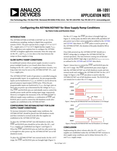
AN-1091
2 Pages
-
AN_737
8 Pages
-
AN-0982
4 Pages
-
ADF7024
24 Pages
-
AD9915
48 Pages
-
AD9914
48 Pages
-
ADRF6612
59 Pages
-
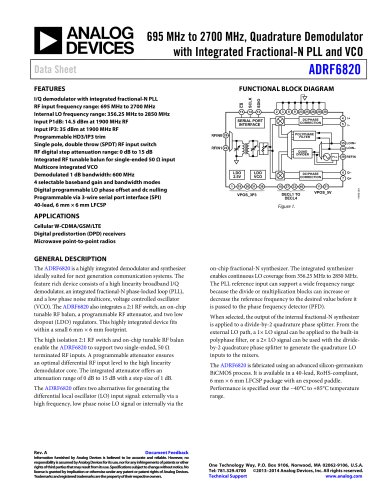
ADRF6820
48 Pages
-
ADL5246
32 Pages
-
ADA4961
22 Pages
-
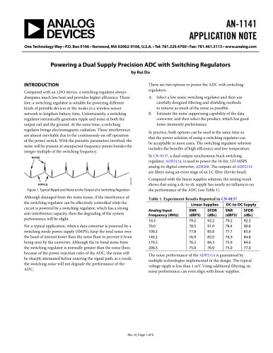
AN-1141
8 Pages
-
AN-698
36 Pages
-
Temperature Sensors
2 Pages
-
Reference Circuits
8 Pages
-
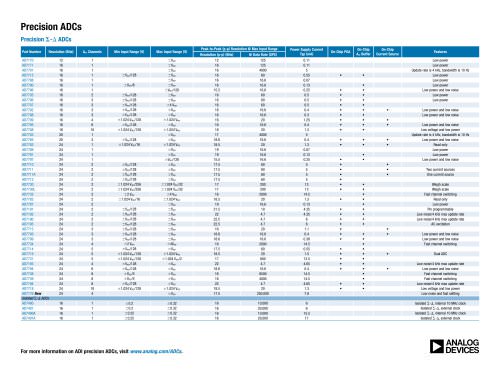
Precision ADCs
16 Pages
-
ADR02ACHIPS: ADR02ACHIPS
8 Pages
-
AD9364 RF Agile Transceiver
32 Pages
-
Digital Temperature Sensors
2 Pages
-
Digital to Analog Converter ICs
12 Pages
-
AD1836A: Multichannel 96 kHz Codec
24 Pages
Archived catalogs
-
Powering ADI Components
8 Pages
-
Zero-Drift Amplifiers
2 Pages


