- Catalogs
- Analog Devices
- ADN2915: Continuous Rate 6.5 Mbps to 11.3 Gbps Clock and Data Recovery IC with Integrated Limiting Amp/EQ
ADN2915: Continuous Rate 6.5 Mbps to 11.3 Gbps Clock and Data Recovery IC with Integrated Limiting Amp/EQ
1 /36Pages

ADN2915: Continuous Rate 6.5 Mbps to 11.3 Gbps Clock and Data Recovery IC with Integrated Limiting Amp/EQ
1 /36Pages
Catalog excerpts
Continuous Rate 6.5 Mbps to 11.3 Gbps Clock and Data Recovery IC with Integrated Limiting Amp/EQ Data Sheet FEATURES GENERAL DESCRIPTION Serial data input: 6.5 Mbps to 11.3 Gbps No reference clock required Exceeds SONET/SDH requirements for jitter transfer/generation/tolerance Quantizer sensitivity: 7.3 mV typical (limiting amplifier mode) Optional limiting amplifier, equalizer, and bypass inputs Programmable jitter transfer bandwidth to support G.8251 OTN Programmable slice level Sample phase adjust (5.65 Gbps or greater) Output polarity invert Programmable LOS threshold via I2C I2C to access optional features Loss of signal (LOS) alarm (limiting amplifier mode only) Loss of lock (LOL) indicator PRBS generator/detector Application-aware power 430 mW at 11.3 Gbps, equalizer enabled, no clock output 380 mW at 6.144 Gbps, limiting amplifier mode, no clock output 340 mW at 622 Mbps, input bypass mode, no clock output Power supply: 1.2 V, flexible 1.8 V to 3.3 V, and 3.3 V 4 mm × 4 mm 24-lead LFCSP The ADN2915 provides the receiver functions of quantization, signal level detect, and clock and data recovery for continuous data rates from 6.5 Mbps to 11.3 Gbps. The ADN2915 automatically locks to all data rates without the need for an external reference clock or programming. ADN2915 jitter performance exceeds all jitter specifications required by SONET/SDH, including jitter transfer, jitter generation, and jitter tolerance. The ADN2915 provides manual or automatic slice adjust and manual sample phase adjusts. Additionally, the user can select a limiting amplifier, equalizer, or bypass at the input. The equalizer is either adaptive or can be manually set. The receiver front-end loss of signal (LOS) detector circuit indicates when the input signal level has fallen below a userprogrammable threshold. The LOS detect circuit has hysteresis to prevent chatter at the LOS output. In addition, the input signal strength can be read through the I2C registers. The ADN2915 also supports pseudorandom binary sequence (PRBS) generation, bit error detection, and input data rate readback features. The ADN2915 is available in a compact 4 mm × 4 mm, 24-lead chip scale package (LFCSP). All ADN2915 specifications are defined over the ambient temperature range of −40°C to +85°C, unless otherwise noted. APPLICATIONS SONET/SDH OC-1/OC-3/OC-12/OC-48/OC-192 and all associated FEC rates 1GFC, 2GFC, 4GFC, 8GFC, 10GFC, 1GE, and 10GE WDM transponders Any rate regenerators/repeaters FUNCTIONAL BLOCK DIAGRAM SCK FREQUENCY ACQUISITION AND LOCK DETECTOR SLICE ADJUST REFCLKP/ REFCLKN (OPTIONAL) DATOUTP/ DATOUTN SAMPLE PHASE ADJUST ÷N DOWNSAMPLER AND LOOP FILTER DATA INPUT SAMPLER DATA RATE CLKOUTP/ CLKOUTN Document Feedback Information furnished by Analog Devices is believed to be accurate and reliable. However, no responsibility is assumed by Analog Devices for its use, nor for any infringements of patents or other rights of third parties that may result from its use. Specifications subject to change without notice. No license is granted by implication or otherwise under any patent or patent rights of Analog Devices. Trademarks and registered trademarks are the property of their respective owners. One Technology Way, P.O. Box 9106, Norwood, MA 02062-9106, U.S.A. Tel: 781.329.4700 ©2013 Analog Devices, Inc. All rights reserved. Technical Support www.analog.com
Open the catalog to page 1
Data Sheet REVISION HISTORY 7/13—Revision 0: Initial Version
Open the catalog to page 2
Data Sheet SPECIFICATIONS TA = TMIN to TMAX, VCC = VCCMIN to VCCMAX, VCC1 = VCC1MIN to VCC1MAX, VDD = VDDMIN to VDDMAX, VEE = 0 V, input data pattern: PRBS 223 − 1, ac-coupled, I2C register default settings, unless otherwise noted. Table 1. Parameter DATA RATE SUPPORT RANGE INPUT—DC CHARACTERISTICS Peak-to-Peak Differential Input 1 Input Resistance BYPASS PATH—CML INPUT Input Voltage Range Input Common-Mode Level Differential Input Sensitivity OC-192 8GFC 2 LIMITING AMPLIFIER INPUT PATH Differential Input Sensitivity OC-48 OC-192 8GFC2 10.3125 Gbps EQUALIZER INPUT PATH Differential Input Sensitivity...
Open the catalog to page 3
2 Fibre Channel Physical Interface 4 standard, FC-P1 -4, Rev 8.00, May 21,2008. 3 When ac-coupled, the LOS assert and deassert times are dominated by the RC time constant of the ac coupling capacitor and the 100 Q differential input termination 4 This typical acquisition specification applies to all selectable reference clock frequencies in the range of 11.05 MHz to 176.8 MHz.
Open the catalog to page 4
Data Sheet JITTER SPECIFICATIONS TA = TMIN to TMAX, VCC = VCCMIN to VCCMAX, VCC1 = VCC1MIN to VCC1MAX, VDD = VDDMIN to VDDMAX, VEE = 0 V, input data pattern: PRBS 223 − 1, ac-coupled to 100 Ω differential termination load, I2C register default settings, unless otherwise noted. Table 2. Parameter PHASE-LOCKED LOOP CHARACTERISTICS Jitter Transfer Bandwidth (BW) 1 OC-192 8GFC 3 OC-48 OC-12 OC-3 Jitter Peaking OC-192 8GFC3 OC-48 OC-12 OC-3 Jitter Generation OC-192 8GFC3 OC-48 8GFC,3 JTSPAT Sinusoidal Jitter at 340 kHz Sinusoidal Jitter at 5.098 MHz Sinusoidal Jitter at 80 MHz Rx Jitter Tracking Test...
Open the catalog to page 5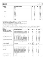
Data Sheet Test Conditions/Comments 600 Hz 6 kHz 100 kHz 1 MHz 20 MHz 30 Hz 300 Hz 25 kHz 250 kHz 5 MHz 30 Hz 300 Hz 6500 Hz 65 kHz 1.3 MHz Jitter transfer bandwidth is programmable by adjusting TRANBW[2:0] in the DPLLA register (0x10). Set TRANBW[2:0] = 1 to enter OTN mode. OTN is the optical transport network as defined in ITU G.709. Fibre Channel Physical Interface 4 standard, FC-P1-4, Rev 8.00, May 21, 2008. 4 Conditions of FC-P1-4, Rev 8.00, Table 27, 800-DF-EL-S apply. 1 2 3 Must have zero errors during the tests for an interval of time that is ≤10−12 BER to pass the tests. OUTPUT AND TIMING...
Open the catalog to page 6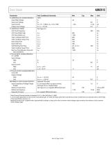
Data Sheet Parameter I2C INTERFACE DC CHARACTERISTICS Input High Voltage Input Low Voltage Input Current Output Low Voltage I2C INTERFACE TIMING SCK Clock Frequency SCK Pulse Width High SCK Pulse Width Low Start Condition Hold Time Start Condition Setup Time Data Setup Time Data Hold Time SCK/SDA Rise/Fall Time Stop Condition Setup Time Bus Free Time Between Stop and Start Conditions LVTTL DC INPUT CHARACTERISITICS (I2C_ADDR) Input Voltage High Low Input Current High Low LVTTL DC OUTPUT CHARACTERISITICS (LOS/LOL) Output Voltage High Low REFERENCE CLOCK CHARACTERISTICS Input Compliance Voltage...
Open the catalog to page 7All Analog Devices catalogs and technical brochures
 HMC722LP3E
8 Pages
 Isolated Sigma-Delta Modulator
17 Pages
 HMC853 Data Sheet
10 Pages
 AN-1084
8 Pages
 AN-1091
2 Pages
 AN_737
8 Pages
 AN-0982
4 Pages
 ADF7024
24 Pages
 AD9915
48 Pages
 AD9914
48 Pages
 ADRF6612
59 Pages
 ADRF6820
48 Pages
 ADL5246
32 Pages
 ADA4961
22 Pages
 AN-1141
8 Pages
 AN-698
36 Pages
 Temperature Sensors
2 Pages
 Reference Circuits
8 Pages
 Precision ADCs
16 Pages
 ADR02ACHIPS: ADR02ACHIPS
8 Pages
 AD9364 RF Agile Transceiver
32 Pages
 Digital Temperature Sensors
2 Pages
 Digital to Analog Converter ICs
12 Pages
 AD1836A: Multichannel 96 kHz Codec
24 Pages


Archived catalogs
 Zero-Drift Amplifiers
2 Pages
 Powering ADI Components
8 Pages


- Ethernet switch
- Industrial network switch
- Acceleration sensor
- Unmanaged switch
- Transceiver module
- Analog Devices motor controller
- Triaxial acceleration sensor
- DC motor controller
- Data acquisition unit
- Analog Devices stepper motor controller
- Industrial converter
- Ethernet transceiver
- Processor
- High-voltage amplifier
- Low-noise amplifier
- Multiplexer
- Compact motor controller
- Gyroscope
- Closed-loop motor controller
- Digital converter