
- Catalogs
- Analog Devices
- ADM690 Functions: 4.65 V Reset, Battery Switchover, Watchdog Timer, Power Fail Input


- Products
- Catalogs
- News & Trends
- Exhibitions
ADM690 Functions: 4.65 V Reset, Battery Switchover, Watchdog Timer, Power Fail Input
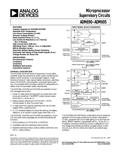
ADM690 Functions: 4.65 V Reset, Battery Switchover, Watchdog Timer, Power Fail Input
Catalog excerpts
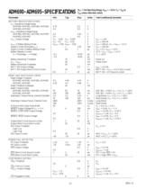
ParameterMinTypMaxUnitsTest Conditions/Comments BATTERY BACKUP SWITCHINGV > CC Operating Voltage RangeADM690, ADM691, ADM694, ADM6954.755.5V ADM692, ADM6934.55.5VV > BATT Operating Voltage RangeADM690, ADM691, ADM694, ADM6952.04.25V ADM692, ADM6932.04.0VV > OUT Output VoltageV > CC 0.05V > CC ֖ 0.025VI > OUT = 1 mAV > CC 0.5V > CC ֖ 0.25VI > OUT ≤ 100 mAV > OUT in Battery Backup ModeV > BATT 0.05V > BATT ֖ 0.02VI > OUT = 250 A, V > CC < V > BATT Ֆ 0.2 VSupply Current (Excludes I > OUT )11.95mAI > OUT = 100 mASupply Current in Battery Backup Mode0.61 AV > CC = 0 V, V > BATT = 2.8 VBattery Standby...
Open the catalog to page 2
ParameterMinTypMaxUnitsTest Conditions/Comments OSCILLATOROSC IN Input Current ֱ 2 AOSC SEL Input Pull-Up Current5 յ AOSC IN Frequency Range0250kHz OSC SEL = 0 V OSC IN Frequency with External Capacitor4kHz OSC SEL = 0 V, C OSC = 47pF NOTE 1 WDI is a three level input which is internally biased to 38% of V CC and has an input impedance of approximately 125 k Ω .Specifications subject to change without notice. ABSOLUTE MAXIMUM RATINGS* ORDERING GUIDE (T A = +25 C unless otherwise noted) V > ModelTemperature RangePackage Option CC . . . . . . . . . . . . . . . . . . . . . . . . . . . . . . . ....
Open the catalog to page 3
PIN FUNCTION DESCRIPTION MnemonicFunction V > CC Power Supply Input: +5 V Nominal.V > BATT Backup Battery Input. Connect to Ground if a backup battery is not used.V > OUT Output Voltage, V > CC or V > BATT is internally switched to V > OUT depending on which is at the highest potential. V > OUT can supply up to 100 mA to power CMOS RAM. Connect V > OUT to V > CC if V > OUT and V > BATT are not used.GND0 V. Ground reference for all signals. RESET Logic Output. RESET goes low if1. V > CC falls below the Reset Threshold2. V > CC falls below V > BATT 3. The watchdog timer is not serviced within its...
Open the catalog to page 4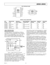
PIN CONFIGURATIONS PRODUCT SELECTION GUIDE BATT 12345678 161514131211109 V OUT RESET ADM691ADM693ADM695 CC V OUT 12348765 ADM690ADM692ADM694 BATT GNDV CC TOP VIEW(Not to Scale) IN BATT ONLOW LINEOSC INOSC SEL RESETCE CE OUT GNDV TOP VIEW(Not to Scale) WDI PFIPFOWDIRESETV PFIPFOWDOV PartNominal ResetNominal V CC Nominal WatchdogBattery BackupBase DriveChip Enable NumberTimeReset ThresholdTimeout PeriodSwitchingExt PNPSignals ADM69050 ms4.65 V1.6 sYesNoNoADM69150 ms or ADJ4.65 V100 ms, 1.6 s, ADJYesYesYesADM69250 ms4.4 V1.6 sYesNoNoADM69350 ms or ADJ4.4 V100 ms, 1.6 s, ADJYesYesYes ADM694200 ms4.65...
Open the catalog to page 5
POWER FAIL RESET OUTPUT Watchdog Timer RESET RESET is an active low output which provides a RESET signalto the Microprocessor whenever V The watchdog timer circuit monitors the activity of the micro-processor in order to check that it is not stalled in an indefiniteloop. An output line on the processor is used to toggle theWatchdog Input (WDI) line. If this line is not toggled within the selected timeout period, a > CC is at an invalid level. WhenV > CC falls below the reset threshold, the RESET output is forcedlow. The nominal reset voltage threshold is 4.65 V (ADM690/ ADM691/ADM694/ADM695)...
Open the catalog to page 6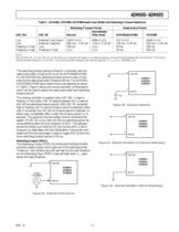
Table I.ADM691, ADM693, ADM695 Reset Pulse Width and Watchdog Timeout Selections Watchdog Timeout Period Reset Active PeriodImmediately OSC SELOSC INNormalAfter ResetADM691/ADM693ADM695 LowExternal Clock Input1024 CLKS4096 CLKS512 CLKS2048 CLKSLowExternal Capacitor260 ms ֗ C/47 pF1.04 s C/47 pF130 ms ח C/47 pF520 ms C/47 pFFloating or HighLow100 ms1.6 s50 ms200 ms Floating or HighFloating or High1.6 s1.6 s50 ms200 ms > NOTEWith the OSC SEL pin low, OSC IN can be driven by an external clock signal, or an external capacitor can be connected between OSC IN and GND. The nominalinternal oscillator...
Open the catalog to page 7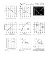
RESET ACTIVE TIME ms PFI INPUT THRESHOLD ֖ V RESET VOLTAGE THRESHOLD V TEMPERATURE ֖
Open the catalog to page 9
CONTROLINPUT*D1D2*LOW = INTERNAL TIMEOUT HIGH = EXTERNAL TIMEOUT V BATT CC PFO ADM69x ֢Ħ LOW BATTERYSIGNAL TO BATTERY20k PFIV ADM69x P I/O PIN+5V INPUTPOWER OSC INOSC SEL 10M բĦ CE Ω IN FROM P I/O PINAPPLIES TEST LOADTO BATTERY OPTIONALTEST LOAD10M CE OUT Figure 20.Monitoring the Battery Status Figure 21b. Programming the Watchdog Input Alternate Watchdog Input Drive Circuits Replacing the Backup Battery The watchdog feature can be enabled and disabled under pro-gram control by driving WDI with a 3-state buffer (Figure 21a).When three-stated, the WDI input will float thereby disabling the watchdog...
Open the catalog to page 11
R =( V > CC ֖ 50 mV )/1 ANote that the resistor will discharge the battery slightly. With aV > +5VV supply of 4.5 V, a suitable resistor is 4.3 M բĦ . With a 3 Vbattery this will draw around 700 nA. This will be negligible inmost cases. > R 1 CC CC P POWER V OUT CMOS RAMPOWERI/O LINE ADM690ADM692ADM694 0.1 յ F R P SYSTEM V 2 BATT յ P RESET RESETWDIGND PFIV BATTERY R ADM69x + BATT PFO P NMI BATTERY Figure 23a.ADM690/ADM692/ADM694 Typical ApplicationCircuit A Figure 22b.Preventing Spurious RESETS During BatteryReplacement Figure 23b shows a similar application but in this case the PFIinput monitors...
Open the catalog to page 12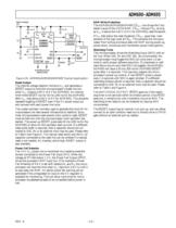
INPUT POWER+5VV RAM Write Protection The ADM691/ADM693/ADM695 CE > OUT line drives the ChipSelect inputs of the CMOS RAM. > 0.1 ֵ F 0.1 F3VBATTERY RESET CE > OUT follows CE > IN as longas V > CC is above the 4.65 V (4.4 V for ADM693) reset threshold.If V > CC BATTON NC V OUT CMOSRAM BATT OUT CC falls below the reset threshold, CE > OUT goes high, inde-pendent of the logic level at > R 1 ADM691ADM693ADM695 CE > IN . This prevents the micropro-cessor from writing erroneous data into RAM during power-up, power-down, brownouts and momentary power interruptions. > CE IN ADDRESSDECODE A0ՖA15 Watchdog...
Open the catalog to page 13All Analog Devices catalogs and technical brochures
 HMC722LP3E
8 Pages
 Isolated Sigma-Delta Modulator
17 Pages
 HMC853 Data Sheet
10 Pages
 AN-1084
8 Pages
 AN-1091
2 Pages
 AN_737
8 Pages
 AN-0982
4 Pages
 ADF7024
24 Pages
 AD9915
48 Pages
 AD9914
48 Pages
 ADRF6612
59 Pages
 ADRF6820
48 Pages
 ADL5246
32 Pages
 ADA4961
22 Pages
 AN-1141
8 Pages
 AN-698
36 Pages
 Temperature Sensors
2 Pages
 Reference Circuits
8 Pages
 Precision ADCs
16 Pages
 ADR02ACHIPS: ADR02ACHIPS
8 Pages
 AD9364 RF Agile Transceiver
32 Pages
 Digital Temperature Sensors
2 Pages
 Digital to Analog Converter ICs
12 Pages
 AD1836A: Multichannel 96 kHz Codec
24 Pages




























Archived catalogs
 Zero-Drift Amplifiers
2 Pages
 Powering ADI Components
8 Pages




- Ethernet switch
- Industrial network switch
- Acceleration sensor
- Unmanaged switch
- Analog Devices motor controller
- Transceiver module
- Triaxial acceleration sensor
- DC motor controller
- Data acquisition unit
- Analog Devices stepper motor controller
- Industrial converter
- Ethernet transceiver
- High-voltage amplifier
- Low-noise amplifier
- Multiplexer
- Compact motor controller
- Digital converter
- Closed-loop motor controller
- Digital motor controller