- Catalogs
- Analog Devices
- ADM1270:High Voltage Input Protection Device
ADM1270:High Voltage Input Protection Device
1 /23Pages

ADM1270:High Voltage Input Protection Device
1 /23Pages
Catalog excerpts
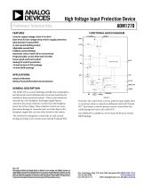
Preliminary Technical Data High Voltage Input Protection Device ADM1270 FEATURES Controls supply voltages from 4 V to 60 V Gate drive for low voltage drop reverse supply protection Gate drive for P-channel FETs In-rush current limiting control Adjustable current limit Foldback current limiting Automatic retry or latch-off on current fault Programmable current-limit timer for SOA Power-good and Fault outputs Analog UV and OV protection 16-lead 3x3mm LFCSP package 16-lead QSOP package FUNCTIONAL BLOCK DIAGRAM VCC/SENSE+ FLB Current Limit FB_PG Current Limit Control GENERAL DESCRIPTION The ADM1270 is designed to control the in-rush current during powering on of a system via an external P-channel FET. Industrial Modules Battery Powered/Portable Instrumentation The ADM1270 is a current limiting controller that is intended to provide inrush current limiting and overcurrent protection for modular or battery powered systems. When circuit boards are inserted into a live backplane, discharged supply bypass capacitors draw large transient currents from the backplane power bus as they charge. These transient currents can cause permanent damage to connector pins, as well as dips on the backplane supply that can reset other boards in the system. To protect the system from a reverse polarity input supply, there is a provision made to control an additional external P-channel FET. This feature is used to prevent reverse current flow that could damage the load or the ADM1270. The ADM1270 is available in a 3x3 16-lead LFCSP and a 16-lead QSOP package. Rev. PrE Information furnished by Analog Devices is believed to be accurate and reliable. However, no responsibility is assumed by Analog Devices for its use, nor for any infringements of patents or other rights of third parties that may result from its use. Specifications subject to change without notice. No license is granted by implication or otherwise under any patent or patent rights of Analog Devices. Trademarks and registered trademarks are the property of their respective owners. One Technology Way, P.O. Box 9106, Norwood, MA 02062-9106, U.S.A. Tel: 781.329.4700 www.analog.com Fax: 781.461.3113 ©2014 Analog Devices, Inc. All rights reserved.
Open the catalog to page 1
Preliminary Technical Data REVISION HISTORY
Open the catalog to page 2
Preliminary Technical Data SPECIFICATIONS VCC/VSENSE+ = 4 V to 60 V, VSENSE = (VSENSE+ − VSENSE−) = 0 V, TA = −40°C to +125°C, unless otherwise noted. Table 1. Parameter POWER SUPPLY Operating Voltage Range Quiescent Current UV PIN Input Current Input Current UV Threshold UV Threshold Hysteresis UV Glitch Filter UV Propagation Delay OV PIN Input Current Input Current OV Threshold OV Threshold Hysteresis OV Glitch Filter OV Propagation Delay SENSE− Input Current VCAP PIN Internally Regulated Voltage Undervoltage Lockout Rising Undervoltage Lockout Falling Undervoltage Hysteresis ISET PIN Reference...
Open the catalog to page 3
Preliminary Technical Data Parameter Foldback Inactive Glitch Filter Duration Response Time TIMER PIN Timer Pull-Up Current Timer High Threshold Timer Low Threshold TIMER_OFF PIN POR Pull-Up Current Retry Pull-Up Current Timer_off High Threshold FOLDBACK (FLB PIN) Input Current Input Current FEEDBK_PG (FB_PG PIN) PWRGD Rising Threshold PWRGD Threshold Hysteresis Input Current Input Current Power-Good Glitch Filter FAULT PIN Output Low Voltage Leakage Current ENABLE PIN Input High Voltage Input Low Voltage Leakage Current PWRGD PIN Output Low Voltage VCC For Valid PWRGD Leakage Current VCBOS VSENSEOC...
Open the catalog to page 4
ABSOLUTE MAXIMUM RATINGS VsENSE (VsENSE+ - VsENSE-) Continuous Current into Any Pin Storage Temperature Range Operating Temperature Range Lead Temperature, Soldering (10 sec) Junction Temperature Stresses above those listed under Absolute Maximum Ratings may cause permanent damage to the device. This is a stress rating only; functional operation of the device at these or any other conditions above those indicated in the operational section of this specification is not implied. Exposure to absolute maximum rating conditions for extended periods may affect device reliability. THERMAL CHARACTERISTICS...
Open the catalog to page 5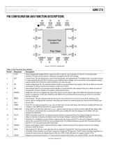
Preliminary Technical Data PIN CONFIGURATION AND FUNCTION DESCRIPTIONS 16 Figure 2. LFCSP Pin Configuration Table 4. Pin Function Descriptions Pin No. 1 Mnemonic VCAP Description Internal Regulated Supply. Place a capacitor with a value of 1 μF or greater on this pin to maintain good accuracy. This pin can be used as a reference to program the ISET pin voltage. Current Limit. This pin allows the current-limit threshold to be programmed. The default limit is set when this pin is connected directly to VCAP. To achieve a user defined sense voltage, the current limit can be adjusted using a resistor...
Open the catalog to page 6
Preliminary Technical Data Pin No. Description current limit. The hot swap operation of the ADM1270 controls the external FET gate to maintain the sense voltage (VSENSE+ − VSENSE−). This pin also connects to the FET drain pin. Positive Supply Input Pin. An undervoltage lockout (UVLO) circuit resets the device when a low supply voltage is detected. GATE is held off when the supply is below UVLO. No sequencing is required. Positive Current Sense Input Pin. This pin connects to the main supply input. A sense resistor between the SENSE+ pin and the SENSE− pin sets the analog current limit. The hot...
Open the catalog to page 7
Preliminary Technical Data Pin No. Description power-up sequence. If this pin is held low, the ADM1270 is prevented from powering up. There is no internal pull-up on this pin. Fault Output. This pin indicates that the device has shut down due to an Over Current fault condition. The device can be configured for automatic retry after shut down by connecting this pin directly to the ENABLE pin. Ground Pin. Timer Pin. An external capacitor, CTIMER, sets an SOA Over Current fault delay. The GATE pin is pulled off when the voltage on the TIMER pin exceeds the upper threshold. Timer Off Pin. An external...
Open the catalog to page 8
Preliminary Technical Data TYPICAL PERFORMANCE CHARACTERISTICS 500 Figure 7. Supply Current (ICC) vs. Temperature, Different Loads Figure 4. VCAP vs. Temperature, Different Loads Figure 8. Supply Current (ICC) vs. Load Current Figure 5. VCAP vs Load Current 3.61 Figure 6. VCAP vs Input Voltage, Different Loads Figure 9. Supply Current (ICC) vs. Supply Voltage (VCC), Different Loads
Open the catalog to page 9All Analog Devices catalogs and technical brochures
 HMC722LP3E
8 Pages
 Isolated Sigma-Delta Modulator
17 Pages
 HMC853 Data Sheet
10 Pages
 AN-1084
8 Pages
 AN-1091
2 Pages
 AN_737
8 Pages
 AN-0982
4 Pages
 ADF7024
24 Pages
 AD9915
48 Pages
 AD9914
48 Pages
 ADRF6612
59 Pages
 ADRF6820
48 Pages
 ADL5246
32 Pages
 ADA4961
22 Pages
 AN-1141
8 Pages
 AN-698
36 Pages
 Temperature Sensors
2 Pages
 Reference Circuits
8 Pages
 Precision ADCs
16 Pages
 ADR02ACHIPS: ADR02ACHIPS
8 Pages
 AD9364 RF Agile Transceiver
32 Pages
 Digital Temperature Sensors
2 Pages
 Digital to Analog Converter ICs
12 Pages
 AD1836A: Multichannel 96 kHz Codec
24 Pages


Archived catalogs
 Zero-Drift Amplifiers
2 Pages
 Powering ADI Components
8 Pages


- Ethernet switch
- Industrial network switch
- Acceleration sensor
- Unmanaged switch
- Transceiver module
- Analog Devices motor controller
- Triaxial acceleration sensor
- DC motor controller
- Data acquisition unit
- Analog Devices stepper motor controller
- Industrial converter
- Ethernet transceiver
- Processor
- High-voltage amplifier
- Low-noise amplifier
- Multiplexer
- Compact motor controller
- Gyroscope
- Closed-loop motor controller
- Digital converter