
- Catalogs
- Analog Devices
- ADL5246


- Products
- Catalogs
- News & Trends
- Exhibitions
ADL5246

ADL5246
The ADL5246 is a versatile RF amplifier module operating up to 3 GHz, featuring a variable gain low noise amplifier (LNA) and an integrated ½ W driver amplifier. It offers a maximum gain of 31.5 dB at 2.2 GHz, a voltage variable attenuation range of 45 dB, a noise figure of 1 dB, and an output IP3 of 37 dBm. The device is housed in a 32-lead LFCSP package and operates on a supply voltage between 3.3 V and 5 V.
Suitable for multistandard radio receivers, point-to-point Rx and Tx, instrumentation, and military and aerospace applications.
Optimized for multistandard base station receivers and point-to-point applications, the ADL5246 includes a low noise amplifier, a high linearity VGA, and a ½ W output driver stage. It can be tuned externally within the 0.6 GHz to 3 GHz range and biased between 3.3 V and 5 V.
At 2.2 GHz, the ADL5246 provides a gain of 11.5 dB, an output 1 dB compression point of 22.3 dBm, and a noise figure of 1 dB. Performance varies with frequency, temperature, and supply voltage.
Maximum supply voltage is 5.5 V, RF input level is 20 dBm, internal power dissipation limit is 3 W, and operational temperature range is -40°C to +105°C.
Thermal resistance is specified as 16.5 °C/W for θJA and 1.15 °C/W for θJC.
The 32-lead configuration includes specific pins for ground, RF input/output, and control voltages. The exposed paddle must be soldered to a low impedance ground plane.
Details basic connections for the ADL5246, with AMP1 as a low noise amplifier, AMP2 as a variable gain amplifier, and AMP3 as a broadband driver. Gain control is managed via VGAIN1 and VGAIN2.
Instructions for matching AMP3 to 50 Ω using external components are provided. Gain control is achieved through integrated VVAs with a voltage range of 0 V to 3.3 V.
Recommendations for PCB land patterns to ensure efficient thermal dissipation, emphasizing the use of thermal vias and proper soldering techniques.
The evaluation board is designed for testing individual amplifiers or cascading them, with specific RF trace characteristics and options for adding filters.
Advises on PCB layout precautions to prevent instability, especially at frequencies below 1.5 GHz, suggesting shielding and minimizing coupling between amplifiers.
- Power Supply Decoupling Capacitors: Specific capacitors for AMP1 and AMP2 are detailed for optimal performance.
- Bias Inductors: Inductors for AMP1 and AMP2 must provide high impedance at operational frequencies.
- Logic Control and Gain Control: Uses resistors and capacitors for isolation and decoupling.
- AC Coupling Capacitors: Specific capacitors for AMP2 and AMP3 are detailed.
- Optional Components: Lists components not installed but available for tuning.
Tested across multiple samples and frequency bands using specialized equipment, with heat management addressed using heat sinks.
Housed in a 32-lead LFCSP package with dimensions provided for integration.
Available in a RoHS compliant package, with an evaluation board option for testing and development.
Catalog excerpts
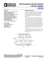
3 GHz Variable Gain LNA with Integrated ½ W Driver Amplifier ADL5246 Data Sheet FEATURES GENERAL DESCRIPTION RF output frequency range: 0.6 GHz to 3 GHz Output IP3: 37 dBm at 2.2 GHz Output P1dB: 28 dBm at 2.2 GHz Noise figure of input amplifier: 1 dB at 2.2 GHz Maximum gain: 31.5 dB at 2.2 GHz Voltage variable attenuation range: 45 dB 0 V to 3.3 V attenuation control range Integrated bypass switch for low noise VGA Matched 50 Ω input stage 3.3 V to 5 V single supply 32-lead, 5 mm × 5 mm LFCSP package The ADL5246 is a high performance, low noise variable gain amplifier (VGA) optimized for multistandard base station receivers and point to point receive (Rx) and transmit (Tx) applications. The low noise figure and excellent linearity performance allow the device to be used in a variety of applications. The device consists of a low noise amplifier, a high linearity VGA, and a ½ W output driver stage. The variable attenuator networks are optimized to provide high linearity performance over the 45 dB gain control range. Gain is set using a unipolar control voltage from 0 V to 3.3 V. The output stage of the ADL5246 is an externally tuned ½ W driver amplifier, which allows the device to be optimized anywhere between the 0.6 GHz to 3 GHz range, with an average tuning bandwidth of 200 MHz wide. An external filter can be used between the VGA and the final driver amplifier. The ADL5246 can be biased between 3.3 V and 5 V to trade-off between performance and power consumption. APPLICATIONS Multistandard radio receivers Point to point Rx and Tx Instrumentation Military and aerospace The ADL5246 is fabricated on an advanced GaAs process. The device is available in a 32-lead, RoHS-compliant, 5 mm × 5 mm LFCSP and thermally rated to operate over the −40°C to +105°C temperature range. FUNCTIONAL BLOCK DIAGRAM Document Feedback Information furnished by Analog Devices is believed to be accurate and reliable. However, no responsibility is assumed by Analog Devices for its use, nor for any infringements of patents or other rights of third parties that may result from its use. Specifications subject to change without notice. No license is granted by implication or otherwise under any patent or patent rights of Analog Devices. Trademarks and registered trademarks are the property of their respective owners. One Technology Way, P.O. Box 9106, Norwood, MA 02062-9106, U.S.A. Tel: 781.329.4700 ©2014 Analog Devices, Inc. All rights reserved. Technical Support www.analog.com
Open the catalog to page 1
Data Sheet REVISION HISTORY 4/14—Revision 0: Initial Version
Open the catalog to page 2
Data Sheet SPECIFICATIONS VPOS = 5 V, TA = 25°C, unless otherwise noted. Amplifier 1 = AMP1, Amplifier 2 = AMP2, and Amplifier 3 = AMP3. Table 1. Parameter OVERALL FUNCTION Frequency Range AMP1 FREQUENCY = 0.75 GHz Gain vs. Frequency vs. Temperature vs. Supply Input Return Loss Output Return Loss Output 1 dB Compression Point Output Third-Order Intercept Noise Figure AMP1 FREQUENCY = 0.9 GHz Gain vs. Frequency vs. Temperature vs. Supply Input Return Loss Output Return Loss Output 1 dB Compression Point Output Third-Order Intercept Noise Figure AMP1 FREQUENCY = 1.5 GHz Gain vs. Frequency vs. Temperature...
Open the catalog to page 3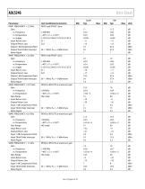
ADL5246 Parameter AMP1 FREQUENCY = 2.2 GHz Gain vs. Frequency vs. Temperature vs. Supply Input Return Loss Output Return Loss Output 1 dB Compression Point Output Third-Order Intercept Noise Figure AMP1 FREQUENCY = 2.6 GHz Gain vs. Frequency vs. Temperature vs. Supply Input Return Loss Output Return Loss Output 1 dB Compression Point Output Third-Order Intercept Noise Figure AMP2 FREQUENCY = 0.75 GHz Gain vs. Frequency vs. Temperature Gain Range Input Return Loss Output Return Loss Input 1 dB Compression Point Input Third-Order Intercept Noise Figure AMP2 FREQUENCY = 0.9 GHz Gain vs. Frequency...
Open the catalog to page 4
Data Sheet Parameter AMP2 FREQUENCY = 1.9 GHz Gain vs. Frequency vs. Temperature Gain Range Input Return Loss Output Return Loss Input 1 dB Compression Point Input Third-Order Intercept Noise Figure AMP2 FREQUENCY = 2.2 GHz Gain vs. Frequency vs. Temperature Gain Range Input Return Loss Output Return Loss Input 1 dB Compression Point Input Third-Order Intercept Noise Figure AMP2 FREQUENCY = 2.6 GHz Gain vs. Frequency vs. Temperature Gain Range Input Return Loss Output Return Loss Input 1 dB Compression Point Input Third-Order Intercept Noise Figure AMP2 GAIN SETTLING Minimum to Maximum Gain Maximum...
Open the catalog to page 5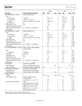
ADL5246 Parameter AMP3 FREQUENCY = 2.2 GHz Gain vs. Frequency vs. Temperature vs. Supply Input Return Loss Output Return Loss Output 1 dB Compression Point Output Third-Order Intercept Noise Figure AMP3 FREQUENCY = 2.6 GHz Gain vs. Frequency vs. Temperature vs. Supply Input Return Loss Output Return Loss Output 1 dB Compression Point Output Third-Order Intercept Noise Figure FULL CHAIN FREQUENCY = 2.2 GHz Gain vs. Frequency Gain Range Input Return Loss Output Return Loss Output 1 dB Compression Point Output Third-Order Intercept Noise Figure LOGIC INPUTS Logic Level Low Logic Level High GAIN...
Open the catalog to page 6
Data Sheet ABSOLUTE MAXIMUM RATINGS Supply Voltage, Vpos Maximum RF Input Level (AMP1) Internal Power Dissipation Maximum Junction Temperature Operating Temperature Range Storage Temperature Range Lead Temperature Range (Soldering 30 sec) Human Body Model (HBM) ESD Rating Stresses at or above those listed under Absolute Maximum Ratings may cause permanent damage to the product. This is a stress rating only; functional operation of the product at these or any other conditions above those indicated in the operational section of this specification is not implied. Operation beyond the maximum operating...
Open the catalog to page 7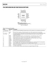
Data Sheet PIN CONFIGURATION AND FUNCTION DESCRIPTIONS NOTES 1. NIC = NO INTERNAL CONNECTION. 2. THE EXPOSED PADDLE (EP) MUST BE SOLDERED TO A LOW IMPEDANCE GROUND PLANE. Description Ground. The exposed paddle (EP) and ground pins must be soldered to a low impedance ground plane. RF Input. This pin requires a dc blocking capacitor. Use a 100 pF capacitor for normal operation. No Internal Connection. These pins are not connected to internal circuitry. The user may optionally solder to a low impedance ground plane for grounding, shielding, and printed circuit board (PCB) trace impedance continuity....
Open the catalog to page 8All Analog Devices catalogs and technical brochures
 HMC722LP3E
8 Pages
 Isolated Sigma-Delta Modulator
17 Pages
 HMC853 Data Sheet
10 Pages
 AN-1084
8 Pages
 AN-1091
2 Pages
 AN_737
8 Pages
 AN-0982
4 Pages
 ADF7024
24 Pages
 AD9915
48 Pages
 AD9914
48 Pages
 ADRF6612
59 Pages
 ADRF6820
48 Pages
 ADA4961
22 Pages
 AN-1141
8 Pages
 AN-698
36 Pages
 Temperature Sensors
2 Pages
 Reference Circuits
8 Pages
 Precision ADCs
16 Pages
 ADR02ACHIPS: ADR02ACHIPS
8 Pages
 AD9364 RF Agile Transceiver
32 Pages
 Digital Temperature Sensors
2 Pages
 Digital to Analog Converter ICs
12 Pages
 AD1836A: Multichannel 96 kHz Codec
24 Pages





























Archived catalogs
 Zero-Drift Amplifiers
2 Pages
 Powering ADI Components
8 Pages




- Ethernet switch
- Industrial network switch
- Acceleration sensor
- Unmanaged switch
- Analog Devices motor controller
- Transceiver module
- Triaxial acceleration sensor
- DC motor controller
- Data acquisition unit
- Analog Devices stepper motor controller
- Industrial converter
- Ethernet transceiver
- Processor
- High-voltage amplifier
- Low-noise amplifier
- Multiplexer
- Compact motor controller
- Digital converter
- Closed-loop motor controller
- Digital motor controller