- Catalogs
- Analog Devices
- ADG3301: Low Voltage 1.15 V to 5.5 V, Single-Channel Bidirectional Logic Level Translator Data Sheet (Rev. 0)
ADG3301: Low Voltage 1.15 V to 5.5 V, Single-Channel Bidirectional Logic Level Translator Data Sheet (Rev. 0)
1 /20Pages

ADG3301: Low Voltage 1.15 V to 5.5 V, Single-Channel Bidirectional Logic Level Translator Data Sheet (Rev. 0)
1 /20Pages
Catalog excerpts
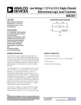
Low Voltage 1.15 V to 5.5 V, Single-Channel Bidirectional Logic Level Translator ADG3301 Bidirectional level translation Operates from 1.15 V to 5.5 V Low quiescent current < 5 µA No direction pin FUNCTIONAL BLOCK DIAGRAM VCCA SPI®, MICROWIRE® level translation Low voltage ASIC level translation Smart card readers Cell phones and cell phone cradles Portable communication devices Telecommunications equipment Network switches and routers Storage systems (SAN/NAS) Computing/server applications GPS Portable POS systems Low cost serial interfaces GENERAL DESCRIPTION PRODUCT HIGHLIGHTS The ADG3301 is a single-channel, bidirectional logic level translator. It can be used in multivoltage digital system applications such as data transfer between a low voltage DSP/controller and a higher voltage device. The internal architecture allows the device to perform bidirectional logic level translation without an additional signal to set the direction in which the translation takes place. 1. Bidirectional level translation. 2. Fully guaranteed over the 1.15 V to 5.5 V supply range. 3. No direction pin. 4. Compact 6-lead SC70 package. The voltage applied to VCCA sets the logic levels on the A side of the device, while VCCY sets the levels on the Y side. For proper operation, VCCA must always be less than VCCY. The VCCAcompatible logic signals applied to the A pin appear as VCCYcompatible levels on the Y pin. Similarly, VCCY-compatible logic levels applied to the Y pin appear as VCCA-compatible logic levels on the A pin. The enable pin (EN) provides three-state operation on both the A pin and the Y pin. When the device enable pin is pulled low, the terminals on both sides of the device are in the high impedance state. The EN pin is referred to the VCCA supply voltage and driven high for normal operation. The ADG3301 is available in a compact 6-lead SC70 package and is guaranteed to operate over the 1.15 V to 5.5 V supply voltage range and extended −40°C to +85°C temperature range. Rev. 0 Information furnished by Analog Devices is believed to be accurate and reliable. However, no responsibility is assumed by Analog Devices for its use, nor for any infringements of patents or other rights of third parties that may result from its use. Specifications subject to change without notice. No license is granted by implication or otherwise under any patent or patent rights of Analog Devices. Trademarks and registered trademarks are the property of their respective owners. One Technology Way, P.O. Box 9106, Norwood, MA 02062-9106, U.S.A. Tel: 781.329.4700 www.analog.com Fax: 781.461.3113 © 2005 Analog Devices, Inc. All rights reserved.
Open the catalog to page 1
REVISION HISTORY 12/05—Revision 0: Initial Version
Open the catalog to page 2
ADG3301 SPECIFICATIONS VCCY = 1.65 V to 5.5 V, VCCA = 1.15 V to VCCY, GND = 0 V. All specifications TMIN to TMAX, unless otherwise noted. Table 1. Parameter1 LOGIC INPUTS/OUTPUTS A Side Input High Voltage3 Input Low Voltage3 Output High Voltage Output Low Voltage Capacitance3 Leakage Current Y Side Input High Voltage3 Input Low Voltage3 Output High Voltage Output Low Voltage Capacitance3 Leakage Current Enable (EN) Input High Voltage3 Input Low Voltage3 Leakage Current Capacitance3 Enable Time3 VIHA VIHA VILA VOHA VOLA CA ILA, HiZ VY = VCCY, IOH = 20 µA, see Figure 27 VY = 0 V, IOL = 20 µA, see...
Open the catalog to page 3
ADG3301 Parameter1 Y→A Translation Propagation Delay Rise Time Fall Time Maximum Data Rate Part-to-Part Skew 1.15 V to 1.3 V ≤ VCCA ≤ VCCY, VCCY = 3.3 V ± 0.3 V A→Y Translation Propagation Delay Rise Time Fall Time Maximum Data Rate Part-to-Part Skew Y→A Translation Propagation Delay Rise Time Fall Time Maximum Data Rate Part-to-Part Skew 1.15 V to 1.3 V ≤ VCCA ≤ VCCY, VCCY = 1.8 V ± 0.3 V A→Y Translation Propagation Delay Rise Time Fall Time Maximum Data Rate Part-to-Part Skew Y→A Translation Propagation Delay Rise Time Fall Time Maximum Data Rate Part-to-Part Skew 2.5 V ± 0.2 V ≤ VCCA ≤ VCCY,...
Open the catalog to page 4
ADG3301 Parameter1 POWER REQUIREMENTS Power Supply Voltages Quiescent Power Supply Current VCCA VCCY ICCA ICCY Three-State Mode Power Supply Current IHiZA IHiZY VA = 0 V/VCCA, VY = 0 V/VCCY, VCCA = VCCY = 5.5 V, EN = 1 VA = 0 V/VCCA, VY = 0 V/VCCY, VCCA = VCCY = 5.5 V, EN = 1 VCCA = VCCY = 5.5 V, EN = 0 VCCA = VCCY = 5.5 V, EN = 0 Temperature range for the B version is −40°C to +85°C. All typical values are at TA = 25°C, unless otherwise noted. Guaranteed by design, not subject to production test.
Open the catalog to page 5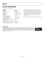
ADG3301 ABSOLUTE MAXIMUM RATINGS TA = 25°C, unless otherwise noted. Table 2. Parameter VCCA to GND VCCY to GND Digital Inputs (A) Digital Inputs (Y) EN to GND Operating Temperature Range Industrial (B Version) Storage Temperature Range Junction Temperature θJA Thermal Impedance (4-Layer Board) 6-Lead SC70 Lead Temperature, Soldering (10 sec) IR Reflow, Peak Temperature (< 20 sec) Rating −0.3 V to +7 V VCCA to +7 V −0.3 V to VCCA + 0.3 V −0.3 V to VCCY + 0.3 V −0.3 V to +7 V −40°C to +85°C −65°C to +150°C 150°C Stresses above those listed under Absolute Maximum Ratings may cause permanent damage...
Open the catalog to page 6
ADG3301 PIN CONFIGURATION AND FUNCTION DESCRIPTIONS VCCA 1 Mnemonic VCCA A GND EN Y VCCY Description Power Supply Voltage Input for the A I/O Pin (1.15 V ≤ VCCA ≤ VCCY). Input/Output A. Referenced to VCCA. Ground (0 V). Active High Enable Input. Input/Output Y. Referenced to VCCY. Power Supply Voltage Input for the Y I/O Pin (1.65 V ≤ VCCY ≤ 5.5V).
Open the catalog to page 7
ADG3301 TYPICAL PERFORMANCE CHARACTERISTICS 3.0 DATA RATE (Mbps) Figure 6. ICCY vs. Data Rate (Y→A Level Translation) Figure 3. ICCA vs. Data Rate (A→Y Level Translation) 1.6 TA = 25°C 1 CHANNEL VCCA = 1.2V VCCY = 1.8V Figure 4. ICCY vs. Data Rate (A→Y Level Translation) Figure 7. ICCY vs. Capacitive Load at Pin Y for A→Y (1.2 V→1.8 V) Level Translation TA = 25°C 1 CHANNEL VCCA = 1.2V VCCY =1.8V VCCA = 1.8V, VCCY = 3.3V VCCA = 1.2V, VCCY = 1.8V DATA RATE (Mbps) Figure 5. ICCA vs. Data Rate (Y→A Level Translation) Figure 8. ICCA vs. Capacitive Load at Pin A for Y→A (1.8 V→1.2 V) Level Translation...
Open the catalog to page 8All Analog Devices catalogs and technical brochures
 HMC722LP3E
8 Pages
 Isolated Sigma-Delta Modulator
17 Pages
 HMC853 Data Sheet
10 Pages
 AN-1084
8 Pages
 AN-1091
2 Pages
 AN_737
8 Pages
 AN-0982
4 Pages
 ADF7024
24 Pages
 AD9915
48 Pages
 AD9914
48 Pages
 ADRF6612
59 Pages
 ADRF6820
48 Pages
 ADL5246
32 Pages
 ADA4961
22 Pages
 AN-1141
8 Pages
 AN-698
36 Pages
 Temperature Sensors
2 Pages
 Reference Circuits
8 Pages
 Precision ADCs
16 Pages
 ADR02ACHIPS: ADR02ACHIPS
8 Pages
 AD9364 RF Agile Transceiver
32 Pages
 Digital Temperature Sensors
2 Pages
 Digital to Analog Converter ICs
12 Pages
 AD1836A: Multichannel 96 kHz Codec
24 Pages


Archived catalogs
 Zero-Drift Amplifiers
2 Pages
 Powering ADI Components
8 Pages


- Industrial network switch
- Acceleration sensor
- Unmanaged switch
- Transceiver module
- Analog Devices motor controller
- Triaxial acceleration sensor
- DC motor controller
- Data acquisition unit
- Analog Devices stepper motor controller
- Industrial converter
- Ethernet transceiver
- Processor
- High-voltage amplifier
- Low-noise amplifier
- Multiplexer
- Compact motor controller
- Gyroscope
- Closed-loop motor controller
- Digital converter