
- Catalogs
- Analog Devices
- ADF4155: Integer-N/Fractional-N PLL Synthesizer


- Products
- Catalogs
- News & Trends
- Exhibitions
ADF4155: Integer-N/Fractional-N PLL Synthesizer
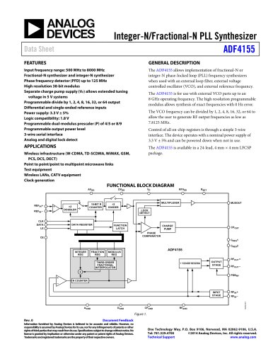
ADF4155: Integer-N/Fractional-N PLL Synthesizer
The ADF4155 is a PLL synthesizer that supports both fractional-N and integer-N modes, with an input frequency range from 500 MHz to 8000 MHz. It includes a phase frequency detector (PFD) up to 125 MHz and a high-resolution 38-bit modulus. The device offers programmable output division and supports differential and single-ended reference inputs. It operates on a 3.3 V ± 5% power supply and is compatible with 1.8 V logic. Key features include a programmable dual-modulus prescaler and a 3-wire serial interface.
The ADF4155 is suitable for use in wireless infrastructure, microwave links, test equipment, wireless LANs, CATV equipment, and clock generation.
The ADF4155 enables the implementation of PLL frequency synthesizers with external components, supporting VCO frequencies up to 8 GHz. It allows for precise frequency synthesis with 0 Hz error and can generate RF output frequencies as low as 7.8125 MHz. The device is controlled via a simple 3-wire interface and can be powered down when not in use. It is available in a compact 24-lead LFCSP package.
The device operates with AVDD, DVDD, and RFVDD at 3.3 V ± 5%, and VP up to 5.5 V. It supports a wide range of input frequencies and offers various programmable features for design flexibility. The charge pump current is adjustable, and the device includes logic inputs and outputs compatible with 1.8 V and 3 V logic levels.
The ADF4155 requires specific timing for its serial interface, with minimum setup and hold times for clock and data signals.
The device has specific voltage and temperature limits to ensure safe operation. Exceeding these limits may cause permanent damage.
The ADF4155 features a detailed pin configuration, with each pin serving specific functions such as serial data input, charge pump output, and RF input/output. Key pins include power supply pins (AVDD, DVDD, RFVDD), control pins (PDBRF), reference input pins (REFIN+ and REFIN−), and ground pins (DGND and EPAD).
Key performance characteristics include RF input sensitivity, charge pump output characteristics, spur levels, and phase noise performance for both integer-N and fractional-N modes.
The document details the reference input section, RF N counter, phase frequency detector and charge pump, and MUXOUT and lock detect functionalities.
The RF output stage is used for lower frequency operation with programmable output power levels. Supply current management allows for shutdown until lock is achieved.
The document provides a summary of registers 0 to 5, detailing their configuration, control bits, and settings for various functions.
Specific integer and fractional value ranges, prescaler settings, and operational limits are provided, along with recommendations for optimizing spurious performance and phase noise.
The document describes the configuration of the antibacklash pulse width and cycle slip reduction settings for optimal performance.
The sequence for initializing the ADF4155 registers is outlined, starting from Register 8 down to Register 0.
An example is provided for programming the ADF4155 synthesizer, including equations for calculating RF frequency output and PFD frequency.
An example application is provided, showing the ADF4155 used with a VCO and RF buffer to produce a local oscillator at 5.8 GHz.
The ADF4155 operates within a temperature range of -40°C to +85°C and is available in a 24-lead LFCSP_WQ package. The document describes procedures for achieving 50 Ω matching and the importance of lock detection in a PLL system.
The document lists different models of the ADF4155 and provides detailed package dimensions, emphasizing proper connection of the exposed pad.
Catalog excerpts
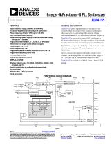
Data Sheet FEATURES GENERAL DESCRIPTION Input frequency range: 500 MHz to 8000 MHz Fractional-N synthesizer and integer-N synthesizer Phase frequency detector (PFD) up to 125 MHz High resolution 38-bit modulus Separate charge pump supply (VP) allows extended tuning voltage in 5 V systems Programmable divide by 1, 2, 4, 8, 16, 32, or 64 output Differential and single-ended reference inputs Power supply: 3.3 V ± 5% Logic compatibility: 1.8 V Programmable dual-modulus prescaler (P) of 4/5 or 8/9 Programmable output power level 3-wire serial interface Analog and digital lock detect The ADF4155 allows implementation of fractional-N or integer-N phase-locked loop (PLL) frequency synthesizers when used with an external loop filter, external voltage controlled oscillator (VCO), and external reference frequency. The ADF4155 is for use with external VCO parts up to an 8 GHz operating frequency. The high resolution programmable modulus allows synthesis of exact frequencies with 0 Hz error. The VCO frequency can be divided by 1, 2, 4, 8, 16, 32, or 64 to allow the user to generate RF output frequencies as low as 7.8125 MHz. Control of all on-chip registers is through a simple 3-wire interface. The device operates with a nominal power supply of 3.3 V ± 5% and can be powered down when not in use. The ADF4155 is available in a 24-lead, 4 mm × 4 mm LFCSP package. Wireless infrastructure (W-CDMA, TD-SCDMA, WiMAX, GSM, PCS, DCS, DECT) Point to point/point to multipoint microwave links Test equipment Wireless LANs, CATV equipment Clock generation FUNCTIONAL BLOCK DIAGRAM AVDD LOCK DETECT DATA REGISTER FUNCTION LATCH CHARGE PUMP PHASE COMPARATOR THIRD-ORDER FRACTIONAL INTERPOLATOR OUTPUT STAGE RFOUT + RFOUT – PDBRF INPUT STAGE Document Feedback Information furnished by Analog Devices is believed to be accurate and reliable. However, no responsibility is assumed by Analog Devices for its use, nor for any infringements of patents or other rights of third parties that may result from its use. Specifications subject to change without notice. No license is granted by implication or otherwise under any patent or patent rights of Analog Devices. Trademarks and registered trademarks are the property of their respective owners. One Technology Way, P.O. Box 9106, Norwood, MA 02062-9106, U.S.A. Tel: 781.329.4700 ©2014 Analog Devices, Inc. All rights reserved. Technical Support www.analog.com
Open the catalog to page 1
Data Sheet REVISION HISTORY 4/14—Revision 0: Initial Version
Open the catalog to page 2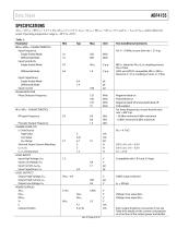
Data Sheet SPECIFICATIONS AVDD = DVDD = RFVDD = 3.3 V ± 5%, AVDD ≤ VP ≤ 5.5 V, AGND = DGND = RFGND = CPGND = 0 V, and TA = TMIN to TMAX, unless otherwise noted. Operating temperature range is −40°C to +85°C. Table 1. Parameter REFIN+\REFIN− CHARACTERISTICS Input Frequency Single-Ended Mode Differential Mode Input Sensitivity Single-Ended Mode Differential Mode For f < 10 MHz, ensure slew rate > 21 V/µs Input Capacitance Single-Ended Mode Differential Mode Input Current PHASE DETECTOR Phase Detector Frequency RFIN+\RFIN− CHARACTERISTICS RF Input Frequency Prescaler Output Frequency CHARGE PUMP...
Open the catalog to page 3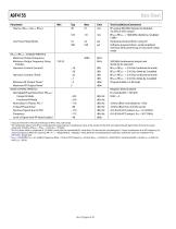
ADF4155 Parameter Total IDD (DIDD + AIDD + RFIDD) RFOUT+/RFOUT− CHARACTERISTICS Maximum Output Frequency Minimum Output Frequency Using Dividers Harmonic Content (Second) Harmonic Content (Third) Minimum RF Output Power 1 Maximum RF Output Power1 NOISE CHARACTERISTICS Normalized Phase Noise Floor, PNSYNTH 2 Integer-N Mode Fractional-N-Mode Normalized 1/f Noise, PN1_f 3 In-Band Phase Noise 4 Spurious Signals due to PFD Frequency Level of Signal with RF Mute Enabled Low Power Sleep Mode dBc/Hz dBc/Hz dBc/Hz dBc/Hz dBc/Hz dBc/Hz dBm Test Conditions/Comments RF output (Bit DB6, Register 6) disabled,...
Open the catalog to page 4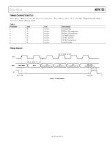
Data Sheet TIMING CHARACTERISTICS AVDD = DVDD = RFVDD = 3.3 V ± 5%, AVDD ≤ VP ≤ 5.5V, AGND = DGND = RFGND = CPGND = 0 V, 1.8 V and 3 V logic levels used, and TA = TMIN to TMAX, unless otherwise noted. Table 2. Parameter t1 t2 t3 t4 t5 t6 t7 Description LE setup time DATA to CLK setup time DATA to CLK hold time CLK high duration CLK low duration CLK to LE setup time LE pulse width Figure 2. Timing Diagram
Open the catalog to page 5
Data Sheet ABSOLUTE MAXIMUM RATINGS TA = 25°C, unless otherwise noted. REFiN+to REFIN— Operating Temperature Range Storage Temperature Range Maximum Junction Temperature Reflow Soldering Charged Device Model Human Body Model Stresses at or above those listed under Absolute Maximum Ratings may cause permanent damage to the product. This is a stress rating only; functional operation of the product at these or any other conditions above those indicated in the operational section of this specification is not implied. Operation beyond the maximum operating conditions for extended periods may affect...
Open the catalog to page 6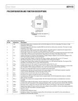
Data Sheet PIN CONFIGURATION AND FUNCTION DESCRIPTIONS NOTES 1. THE EXPOSED PAD MUST BE CONNECTED TO GROUND. Table 4. Pin Function Descriptions Pin No. 1 CPGND AVDD RFIN+ RFIN− AGND RFGND RFOUT− PDBRF DVDD REFIN+ REFIN− MUXOUT Description Serial Clock Input. Data is clocked into the 32-bit shift register on the CLK rising edge. This input is a high impedance CMOS input. Serial Data Input. The serial data is loaded MSB first with the four LSBs as the control bits. This input is a high impedance CMOS input. Load Enable Input. When LE goes high, the data stored in the shift register is loaded into...
Open the catalog to page 7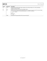
DGND RSET Data Sheet Description Output of Internal LDO. Supply voltage to digital circuits. Nominal voltage of 1.8 V. 100 nF decoupling capacitors to ground required. Digital Ground. Ground return pins for the digital circuitry. Connect a resistor between this pin and ground to set the charge pump output current. The nominal voltage bias at the RSET pin is 0.55 V. The relationship between ICP_MAX and RSET is as follows: ICP_MAX = 23.5/RSET where: RSET = 4.7 kΩ. ICP = 5 mA. Exposed Pad. The exposed pad must be connected to ground.
Open the catalog to page 8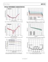
Data Sheet TYPICAL PERFORMANCE CHARACTERISTICS 10 Figure 4. RF Input Sensitivity vs. RF Input Frequency, RF Output Disabled 0 Figure 7. Charge Pump Output Characteristics, VP = 5 V, Selected ICP Values Between 0.312 mA (Minimum) and 5.000 mA (Maximum), RSET = 4.7 kΩ 10 8 2.500mA UP 2.500mA DOWN 3.125mA UP 3.125mA DOWN 4.062mA UP 4.062mA DOWN 0.312mA UP 0.312mA DOWN 0.937mA UP 0.937mA DOWN 1.562mA UP 1.562mA DOWN Figure 5. RF Input Sensitivity vs. RF Input Frequency, RF Output Enabled, RF Divide-by-2 Selected Figure 8. Charge Pump Output Mismatch vs. VCP, Selected ICP Values Between 0.312 mA (Minimum)...
Open the catalog to page 9All Analog Devices catalogs and technical brochures
 HMC722LP3E
8 Pages
 Isolated Sigma-Delta Modulator
17 Pages
 HMC853 Data Sheet
10 Pages
 AN-1084
8 Pages
 AN-1091
2 Pages
 AN_737
8 Pages
 AN-0982
4 Pages
 ADF7024
24 Pages
 AD9915
48 Pages
 AD9914
48 Pages
 ADRF6612
59 Pages
 ADRF6820
48 Pages
 ADL5246
32 Pages
 ADA4961
22 Pages
 AN-1141
8 Pages
 AN-698
36 Pages
 Temperature Sensors
2 Pages
 Reference Circuits
8 Pages
 Precision ADCs
16 Pages
 ADR02ACHIPS: ADR02ACHIPS
8 Pages
 AD9364 RF Agile Transceiver
32 Pages
 Digital Temperature Sensors
2 Pages
 Digital to Analog Converter ICs
12 Pages
 AD1836A: Multichannel 96 kHz Codec
24 Pages


























Archived catalogs
 Zero-Drift Amplifiers
2 Pages
 Powering ADI Components
8 Pages




- Ethernet switch
- Industrial network switch
- Acceleration sensor
- Unmanaged switch
- Analog Devices motor controller
- Transceiver module
- Triaxial acceleration sensor
- DC motor controller
- Data acquisition unit
- Analog Devices stepper motor controller
- Industrial converter
- Ethernet transceiver
- Processor
- High-voltage amplifier
- Low-noise amplifier
- Multiplexer
- Compact motor controller
- Digital converter
- Closed-loop motor controller
- Digital motor controller