
- Catalogs
- Analog Devices
- ADA4932-1/ADA4932-2: Low Power Differential ADC Driver Data Sheet


- Products
- Catalogs
- News & Trends
- Exhibitions
ADA4932-1/ADA4932-2: Low Power Differential ADC Driver Data Sheet
ADA4932-1/ADA4932-2: Low Power Differential ADC Driver Data Sheet
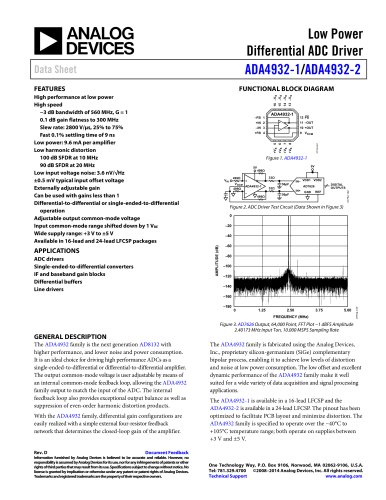
The ADA4932-1/ADA4932-2 are high-performance, low-power differential ADC drivers. They offer a -3 dB bandwidth of 560 MHz at a gain of 1, low harmonic distortion with 100 dB SFDR at 10 MHz, and low input voltage noise of 3.6 nV/√Hz. These devices support both differential-to-differential and single-ended-to-differential operations, with adjustable output common-mode voltage. They operate over a supply range from +3 V to ±5 V and are available in 16-lead and 24-lead LFCSP packages.
These drivers are ideal for ADC drivers, single-ended-to-differential converters, IF and baseband gain blocks, differential buffers, and line drivers.
The ADA4932 family is an advanced version of the AD8132, offering improved performance with lower noise and power consumption. It is designed for driving high-performance ADCs and features an internal common-mode feedback loop for output balance and harmonic distortion suppression. The devices are fabricated using a proprietary silicon-germanium (SiGe) process.
- ±5 V Operation: -3 dB small signal bandwidth of 560 MHz, slew rate of 2800 V/µs, low input offset voltage of ±0.5 mV, and quiescent current of 9.6 mA per amplifier.
- 5 V Operation: Similar performance with slight variations in bandwidth and slew rate.
Maximum supply voltage is 11 V, operating temperature range is -40°C to +105°C, input currents of ±5 mA, and junction temperature limit of 150°C.
Guidance on setting closed-loop gain, estimating output noise voltage, and managing feedback network mismatches. Covers input and output capacitive AC coupling and setting the output common-mode voltage.
Recommendations for optimal PCB layout to minimize distortion and ensure stable operation.
Thermal resistance (θJA) for ADA4932-1 is 91 °C/W, and for ADA4932-2 is 65 °C/W, when soldered to a high thermal conductivity 2s2p circuit board.
Limited by junction temperature rise on the die. Exceeding 150°C can affect performance and cause failure. Power dissipation is the sum of quiescent power and load drive power.
Detailed pin configurations for ADA4932-1 and ADA4932-2, including descriptions for each pin's function.
Graphs illustrate frequency response under various conditions, helping understand device behavior in different scenarios.
Figures show harmonic distortion versus frequency for different loads, supply voltages, and gains. Spurious-free dynamic range is also depicted.
Characteristics such as CMRR, PSRR, output balance, return loss, voltage noise spectral density, and crosstalk are presented through graphs.
The ADA4932 family is a differential amplifier with two outputs moving in opposite directions and an additional VOCM input. It uses high open-loop gain and negative feedback to control output voltages.
Operates similarly to a standard op amp, facilitating single-ended-to-differential conversions and common-mode level shifting. Employs two feedback loops for balanced outputs over a wide frequency range.
Application circuits analyzed by assuming zero differential and common-mode error voltages. Closed-loop gain determined by feedback resistors ratio. Output noise voltage estimated using a noise model.
Input impedance varies with signal source type. Proper termination involves matching source resistance with a termination resistor.
Resistor mismatches can degrade CMRR and introduce offsets. Using 1% tolerance resistors minimizes these effects.
Designed for dual and single-supply applications. Input common-mode range specified for ±5 V and +5 V operations.
Best suited for dc-coupled applications but can be used in ac-coupled circuits.
VOCM pin is internally biased, with external source or resistor divider recommended for more accurate control.
Used to drive AD7626 ADC with a 2.4 MHz band-pass filter to eliminate harmonics.
Configured with a single 3.3 V supply and a gain of 1 for single-ended input to differential output.
Requires a solid ground plane and careful PCB design to realize performance.
Provides detailed dimensions for ADA4932 packages and an ordering guide for different models and quantities.
Catalog excerpts

Low Power Differential ADC Driver ADA4932-1/ADA4932-2 Data Sheet ADC drivers Single-ended-to-differential converters IF and baseband gain blocks Differential buffers Line drivers DIGITAL OUTPUTS Figure 2. ADC Driver Test Circuit (Data Shown in Figure 3) 0 –20 –40 AMPLITUDE (dB) FUNCTIONAL BLOCK DIAGRAM High performance at low power High speed −3 dB bandwidth of 560 MHz, G = 1 0.1 dB gain flatness to 300 MHz Slew rate: 2800 V/μs, 25% to 75% Fast 0.1% settling time of 9 ns Low power: 9.6 mA per amplifier Low harmonic distortion 100 dB SFDR at 10 MHz 90 dB SFDR at 20 MHz Low input voltage noise: 3.6 nV/√Hz ±0.5 mV typical input offset voltage Externally adjustable gain Can be used with gains less than 1 Differential-to-differential or single-ended-to-differential operation Adjustable output common-mode voltage Input common-mode range shifted down by 1 VBE Wide supply range: +3 V to ±5 V Available in 16-lead and 24-lead LFCSP packages Figure 3. AD7626 Output, 64,000 Point, FFT Plot −1 dBFS Amplitude 2.40173 MHz Input Ton, 10.000 MSPS Sampling Rate GENERAL DESCRIPTION The ADA4932 family is the next generation AD8132 with higher performance, and lower noise and power consumption. It is an ideal choice for driving high performance ADCs as a single-ended-to-differential or differential-to-differential amplifier. The output common-mode voltage is user adjustable by means of an internal common-mode feedback loop, allowing the ADA4932 family output to match the input of the ADC. The internal feedback loop also provides exceptional output balance as well as suppression of even-order harmonic distortion products. With the ADA4932 family, differential gain configurations are easily realized with a simple external four-resistor feedback network that determines the closed-loop gain of the amplifier. The ADA4932 family is fabricated using the Analog Devices, Inc., proprietary silicon-germanium (SiGe) complementary bipolar process, enabling it to achieve low levels of distortion and noise at low power consumption. The low offset and excellent dynamic performance of the ADA4932 family make it well suited for a wide variety of data acquisition and signal processing applications. The ADA4932-1 is available in a 16-lead LFCSP and the ADA4932-2 is available in a 24-lead LFCSP. The pinout has been optimized to facilitate PCB layout and minimize distortion. The ADA4932 family is specified to operate over the −40°C to +105°C temperature range; both operate on supplies between +3 V and ±5 V. Document Feedback Information furnished by Analog Devices is believed to be accurate and reliable. However, no responsibility is assumed by Analog Devices for its use, nor for any infringements of patents or other rights of third parties that may result from its use. Specifications subject to change without notice. No license is granted by implication or otherwise under any patent or patent rights of Analog Devices. Trademarks and registered trademarks are the property of their respective owners. One Technology Way, P.O. Box 9106, Norwood, MA 02062-9106, U.S.A. Tel: 781.329.4700 ©2008–2014 Analog Devices, Inc. All rights reserved. Technical Support www.analog.com
Open the catalog to page 1
Data Sheet REVISION HISTORY
Open the catalog to page 2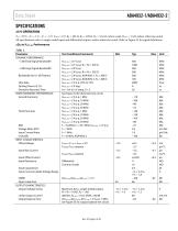
Data Sheet SPECIFICATIONS ±5 V OPERATION TA = 25°C, +VS = 5 V, −VS = −5 V, VOCM = 0 V, RF = 499 Ω, RG = 499 Ω, RT = 53.6 Ω (when used), RL, dm = 1 kΩ, unless otherwise noted. All specifications refer to single-ended input and differential outputs, unless otherwise noted. Refer to Figure 55 for signal definitions. ±DIN to VOUT, dm Performance Table 1. Parameter DYNAMIC PERFORMANCE −3 dB Small Signal Bandwidth −3 dB Large Signal Bandwidth Bandwidth for 0.1 dB Flatness Slew Rate Settling Time to 0.1% Overdrive Recovery Time NOISE/HARMONIC PERFORMANCE Second Harmonic Third Harmonic IMD Voltage Noise...
Open the catalog to page 3
Data Sheet VOCM to VOUT, cm Performance Table 2. Parameter VOCM DYNAMIC PERFORMANCE −3 dB Small Signal Bandwidth −3 dB Large Signal Bandwidth Slew Rate Input Voltage Noise (RTI) VOCM INPUT CHARACTERISTICS Input Voltage Range Input Resistance Input Offset Voltage VOCM CMRR Gain Test Conditions/Comments V+DIN = V−DIN = 0 V ΔVOUT, dm/ΔVOCM, ΔVOCM = ±1 V ΔVOUT, cm/ΔVOCM, ΔVOCM = ±1 V General Performance Table 3. Parameter POWER SUPPLY Operating Range Quiescent Current per Amplifier Power Supply Rejection Ratio POWER-DOWN (PD) PD Input Voltage Turn-Off Time Turn-On Time PD Pin Bias Current per Amplifier...
Open the catalog to page 4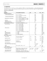
Data Sheet 5 V OPERATION TA = 25°C, +VS = 5 V, −VS = 0 V, VOCM = 2.5 V, RF = 499 Ω, RG = 499 Ω, RT = 53.6 Ω (when used), RL, dm = 1 kΩ, unless otherwise noted. All specifications refer to single-ended input and differential outputs, unless otherwise noted. Refer to Figure 55 for signal definitions. ±DIN to VOUT, dm Performance Table 4. Parameter DYNAMIC PERFORMANCE −3 dB Small Signal Bandwidth −3 dB Large Signal Bandwidth Bandwidth for 0.1 dB Flatness Slew Rate Settling Time to 0.1% Overdrive Recovery Time NOISE/HARMONIC PERFORMANCE Second Harmonic Third Harmonic IMD Voltage Noise (RTI) Input...
Open the catalog to page 5
Data Sheet VOCM to VOUT, cm Performance Table 5. Parameter VOCM DYNAMIC PERFORMANCE −3 dB Small Signal Bandwidth −3 dB Large Signal Bandwidth Slew Rate Input Voltage Noise (RTI) VOCM INPUT CHARACTERISTICS Input Voltage Range Input Resistance Input Offset Voltage VOCM CMRR Gain Test Conditions/Comments V+DIN = V−DIN = 2.5 V ΔVOUT, dm/ΔVOCM, ΔVOCM = ±1 V ΔVOUT, cm/ΔVOCM, ΔVOCM = ±1 V General Performance Table 6. Parameter POWER SUPPLY Operating Range Quiescent Current per Amplifier Power Supply Rejection Ratio POWER-DOWN (PD) PD Input Voltage Turn-Off Time Turn-On Time PD Pin Bias Current per Amplifier...
Open the catalog to page 6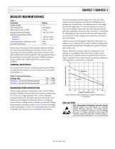
Data Sheet ABSOLUTE MAXIMUM RATINGS Parameter Supply Voltage Power Dissipation Input Current, +IN, −IN, PD Storage Temperature Range Operating Temperature Range ADA4932-1 ADA4932-2 Lead Temperature (Soldering, 10 sec) Junction Temperature Stresses above those listed under Absolute Maximum Ratings may cause permanent damage to the device. This is a stress rating only; functional operation of the device at these or any other conditions above those indicated in the operational section of this specification is not implied. Exposure to absolute maximum rating conditions for extended periods may affect...
Open the catalog to page 7All Analog Devices catalogs and technical brochures
 HMC722LP3E
8 Pages
 Isolated Sigma-Delta Modulator
17 Pages
 HMC853 Data Sheet
10 Pages
 AN-1084
8 Pages
 AN-1091
2 Pages
 AN_737
8 Pages
 AN-0982
4 Pages
 ADF7024
24 Pages
 AD9915
48 Pages
 AD9914
48 Pages
 ADRF6612
59 Pages
 ADRF6820
48 Pages
 ADL5246
32 Pages
 ADA4961
22 Pages
 AN-1141
8 Pages
 AN-698
36 Pages
 Temperature Sensors
2 Pages
 Reference Circuits
8 Pages
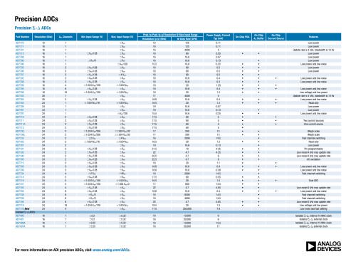
 Precision ADCs
16 Pages
 ADR02ACHIPS: ADR02ACHIPS
8 Pages
 AD9364 RF Agile Transceiver
32 Pages
 Digital Temperature Sensors
2 Pages
 Digital to Analog Converter ICs
12 Pages
 AD1836A: Multichannel 96 kHz Codec
24 Pages




























Archived catalogs
 Zero-Drift Amplifiers
2 Pages
 Powering ADI Components
8 Pages




- Ethernet switch
- Industrial network switch
- Acceleration sensor
- Unmanaged switch
- Analog Devices motor controller
- Transceiver module
- Triaxial acceleration sensor
- DC motor controller
- Data acquisition unit
- Analog Devices stepper motor controller
- Industrial converter
- Ethernet transceiver
- Processor
- High-voltage amplifier
- Low-noise amplifier
- Multiplexer
- Compact motor controller
- Digital converter
- Closed-loop motor controller
- Digital motor controller