- Catalogs
- Analog Devices
- ADA4177-2: OVP and EMI Protected, Precision, Low Noise and Bias Current Op Amp Data Sheet
ADA4177-2: OVP and EMI Protected, Precision, Low Noise and Bias Current Op Amp Data Sheet
1 /25Pages

ADA4177-2: OVP and EMI Protected, Precision, Low Noise and Bias Current Op Amp Data Sheet
1 /25Pages
Catalog excerpts

OVP and EMI Protected, Precision, Low Noise and Bias Current Op Amp ADA4177-2 Data Sheet PIN CONNECTION DIAGRAM OUT A 1 TOP VIEW (Not to Scale) Applications for this amplifier include sensor signal conditioning (such as thermocouples, RTDs, and strain gages), process control front-end amplifiers, and precision diode power measurement in optical and wireless transmission systems. The ADA4177-2 is useful in line powered and portable instrumentation, precision filters, and voltage or current measurement and level setting. The ADA4177-2 operates over the −40°C to +125°C industrial temperature range. The ADA4177-2 is available in an 8-lead SOIC package and an 8-lead MSOP package. 12 10 8 APPLICATIONS Wireless base station control circuits Optical network control circuits Instrumentation Sensors and controls Thermocouples, resistor thermal detectors (RTDs), strain gages, shunt current measurements Precision filters Figure 2. Overvoltage Current Limiting, Voltage Follower Configuration GENERAL DESCRIPTION The ADA4177-2 is a dual-channel amplifier featuring low offset voltage (2 µV typical) and drift (1 µV/°C maximum), and low input bias current, noise, and current consumption (500 µA typical). Outputs are stable with capacitive loads of more than 1000 pF with no external compensation. Table 1. Evolution of Protected Input Op Amps by Generation 1 Gen. 1, OVP (10 V) OP291 OP491 The ADA4177-2 inputs set a new standard in precision amplifier robustness providing input protection against signal excursions 32 V beyond either supply, as well as 70 dB of rejection for electromagnetic interference (EMI) at 1000 MHz. 1 INPUT BIAS CURRENT (mA) Low offset voltage: 60 µV maximum at 25°C (8-lead SOIC) Low offset voltage drift: 1 µV/°C maximum Low input bias current: 1 nA maximum at 25°C Low voltage noise density: 8 nV/√Hz typical Large signal voltage gain (AVO): 100 dB minimum over full supply voltage and operating temperature Input overvoltage protection to 32 V above and below the supply voltage rail Integrated EMI filter 70 dB typical rejection at 1000 MHz 90 dB typical rejection at 2400 MHz Rail-to-rail output swing Low supply current: 500 µA typical per amplifier Wide bandwidth Gain bandwidth product (AV = +100): 3.5 MHz typical Unity-gain crossover: 3.5 MHz typical −3 dB bandwidth (AV = +1): 6 MHz typical Dual-supply operation Specified at ±5 V to ±15 V Operates over ±2.5 V to ±18 V Unity-gain stable No phase reversal Document Feedback Information furnished by Analog Devices is believed to be accurate and reliable. However, no responsibility is assumed by Analog Devices for its use, nor for any infringements of patents or other rights of third parties that may result from its use. Specifications subject to change without notice. No license is granted by implication or otherwise under any patent or patent rights of Analog Devices. Trademarks and registered trademarks are the property of their respective owners. One Technology Way, P.O. Box 9106, Norwood, MA 02062-9106, U.S.A. Tel: 781.329.4700 ©2014 Analog Devices, Inc. All rights reserved. Technical Support www.analog.com
Open the catalog to page 1
Data Sheet Limiting Overvoltage Current Out of the Positive Supply Pin.. 22
Open the catalog to page 2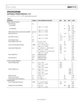
Data Sheet SPECIFICATIONS ELECTRICAL CHARACTERISTICS, ±5 V VSY = ±5.0 V, VCM = 0 V, TA = 25°C, unless otherwise noted. Table 2. Parameter INPUT CHARACTERISTICS Offset Voltage 8-Lead SOIC Test Conditions/Comments 8-Lead MSOP Offset Voltage Drift (8-Lead SOIC/8-Lead MSOP) Input Bias Current Input Offset Current Input Voltage Range Overvoltage Current Limit 1 Common-Mode Rejection Ratio Large Signal Voltage Gain Input Capacitance Input Resistance OUTPUT CHARACTERISTICS Output Voltage High Output Current Short-Circuit Current Closed-Loop Output Impedance POWER SUPPLY Power Supply Rejection Ratio...
Open the catalog to page 3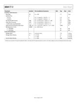
ADA4177-2 Parameter DYNAMIC PERFORMANCE Slew Rate Settling Time To 0.1% To 0.01% Gain Bandwidth Product Unity-Gain Crossover −3 dB Closed-Loop Bandwidth Total Harmonic Distortion Plus Noise EMI Rejection of +IN x f = 1000 MHz f = 2400 MHz NOISE PERFORMANCE Voltage Noise Voltage Noise Density Current Noise Density 1 Data Sheet Symbol Test Conditions/Comments nV p-p nV/√Hz nV/√Hz pA/√Hz All inputs are stressed to 32 V beyond supplies for 500 ms. See Figure 64 for the typical input bias current vs. the input voltage over the overvoltage protected input range.
Open the catalog to page 4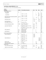
Data Sheet ELECTRICAL CHARACTERISTICS, ±15 V VSY = ±15 V, VCM = 0 V, TA = 25°C, unless otherwise noted. Table 3. Parameter INPUT CHARACTERISTICS Offset Voltage 8-Lead SOIC Test Conditions/Comments 8-Lead MSOP Offset Voltage Drift (8-Lead SOIC/8-Lead MSOP) Input Bias Current Input Offset Current Input Voltage Range Overvoltage Current Limit 1 Common-Mode Rejection Ratio Large Signal Voltage Gain Input Capacitance Input Resistance OUTPUT CHARACTERISTICS Output Voltage High Output Current Short-Circuit Current Closed-Loop Output Impedance POWER SUPPLY Power Supply Rejection Ratio Supply Current...
Open the catalog to page 5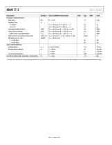
ADA4177-2 Parameter DYNAMIC PERFORMANCE Slew Rate Settling Time To 0.01% To 0.1% Gain Bandwidth Product Unity-Gain Crossover −3 dB Closed-Loop Bandwidth Total Harmonic Distortion Plus Noise EMI Rejection of +IN x f = 1000 MHz f = 2400 MHz NOISE PERFORMANCE Voltage Noise Voltage Noise Density Current Noise Density MULTIPLE AMPLIFIERS CHANNEL SEPARATION 1 Data Sheet Symbol Test Conditions/Comments nV p-p nV/√Hz nV/√Hz pA/√Hz dB All inputs are stressed to 32 V beyond supplies for 500 ms. See Figure 67 for the typical input bias current vs. the input voltage over the overvoltage protected input range....
Open the catalog to page 6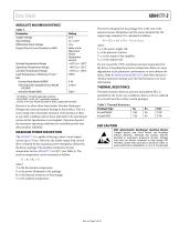
Data Sheet ABSOLUTE MAXIMUM RATINGS Supply Voltage Differential InputVoltage Output Short-Circuit Duration to GND Storage Temperature Range Operating Temperature Range Junction Temperature Range Lead Temperature, Soldering (10 sec)1 Human Body Model (HBM)2 Field Induced Charged Device Model ' IPC/JEDEC J-STS-020D applicable standard. 2 ESDA/JEDEC JS-001-2011 applicable standard. 3 JESD22-C101 (ESD FICDM standard of JEDEC) applicable standard. Stresses at or above those listed under Absolute Maximum Ratings may cause permanent damage to the product. This is a stress rating only; functional operation...
Open the catalog to page 7All Analog Devices catalogs and technical brochures
 HMC722LP3E
8 Pages
 Isolated Sigma-Delta Modulator
17 Pages
 HMC853 Data Sheet
10 Pages
 AN-1084
8 Pages
 AN-1091
2 Pages
 AN_737
8 Pages
 AN-0982
4 Pages
 ADF7024
24 Pages
 AD9915
48 Pages
 AD9914
48 Pages
 ADRF6612
59 Pages
 ADRF6820
48 Pages
 ADL5246
32 Pages
 ADA4961
22 Pages
 AN-1141
8 Pages
 AN-698
36 Pages
 Temperature Sensors
2 Pages
 Reference Circuits
8 Pages
 Precision ADCs
16 Pages
 ADR02ACHIPS: ADR02ACHIPS
8 Pages
 AD9364 RF Agile Transceiver
32 Pages
 Digital Temperature Sensors
2 Pages
 Digital to Analog Converter ICs
12 Pages
 AD1836A: Multichannel 96 kHz Codec
24 Pages


Archived catalogs
 Zero-Drift Amplifiers
2 Pages
 Powering ADI Components
8 Pages


- Ethernet switch
- Industrial network switch
- Acceleration sensor
- Unmanaged switch
- Transceiver module
- Analog Devices motor controller
- Triaxial acceleration sensor
- DC motor controller
- Data acquisition unit
- Analog Devices stepper motor controller
- Industrial converter
- Ethernet transceiver
- Processor
- High-voltage amplifier
- Low-noise amplifier
- Multiplexer
- Compact motor controller
- Gyroscope
- Closed-loop motor controller
- Digital converter