- Catalogs
- Analog Devices
- AD9993: Integrated Mixed-Signal Front End (MxFE) Data Sheet
AD9993: Integrated Mixed-Signal Front End (MxFE) Data Sheet
1 /56Pages

AD9993: Integrated Mixed-Signal Front End (MxFE) Data Sheet
1 /56Pages
Catalog excerpts
Integrated Mixed-Signal Front End (MxFE) AD9993 Data Sheet FEATURES GENERAL DESCRIPTION Quad 14-bit 250 MSPS ADC SFDR = 83 dBc at 87 MHz input Dual 14-bit 500 MSPS DAC SFDR = 75 dBc at 20 MHz output On-chip PLL clock synthesizer Low power 1536 mW, 1 GHz master clock, on-chip synthesizer 500 MHz double data rate (DDR) LVDS interfaces for DACs and ADCs Small 12 mm × 12 mm lead-free BGA package The AD9993 is a mixed-signal front-end (MxFE®) device that integrates four 14-bit ADCs and two 14-bit DACs. Figure 1 shows the block diagram of the MxFE. The MxFE is programmable using registers accessed via a serial peripheral interface (SPI). ADC and DAC datapaths include FIFO buffers to absorb phase differences between LVDS lane clocks and the data converter sampling clocks. The MxFE DACs are part of the Analog Devices, Inc., high speed CMOS DAC core family. These DACs are designed to be used in wide bandwidth communication system transmitter (Tx) signal chains. Point to point microwave backhaul radios Wireless repeaters The MxFE ADCs are multistage pipelined CMOS ADC cores designed for use in communications receivers. FUNCTIONAL BLOCK DIAGRAM 2 LVDS BUFFER –ADC AND DAC DATAPATHS –CONTROLS –SPI REGISTERS –FIFO BUFFERS SPI_SCLK, SPI_CS, SPI_SDI, SPI_SDO RST CLOCK GENERATOR Document Feedback Information furnished by Analog Devices is believed to be accurate and reliable. However, no responsibility is assumed by Analog Devices for its use, nor for any infringements of patents or other rights of third parties that may result from its use. Specifications subject to change without notice. No license is granted by implication or otherwise under any patent or patent rights of Analog Devices. Trademarks and registered trademarks are the property of their respective owners. One Technology Way, P.O. Box 9106, Norwood, MA 02062-9106, U.S.A. Tel: 781.329.4700 ©2014 Analog Devices, Inc. All rights reserved. Technical Support www.analog.com
Open the catalog to page 1
Data Sheet Align ADC LVDS Clocks, ADC FIFO, DAC FIFO Register 32
Open the catalog to page 2
Data Sheet Bits[15:8] of Temperature Sensor Data Readback Register ... 49
Open the catalog to page 3
Data Sheet SPECIFICATIONS DC SPECIFICATIONS TMIN to TMAX, AVDD33 = 3.3 V, DVDD = AVDD = 1.8 V, unless otherwise noted. Table 1. Parameter Tx DAC RESOLUTION Tx DAC OUTPUT CHARACTERISTICS Offset Error Gain Error Full-Scale Output Current (IOUTFS) Output Compliance Voltage Range Output Compliance Voltage Range Output Resistance Tx DAC TEMPERATURE DRIFT Gain Reference Voltage (VREF_DAC) REFERENCE (VREF_DAC) Internal Reference Voltage Rx ADC RESOLUTION Rx ADC CHARACTERISTICS Gain Error Peak-to-Peak Differential Input Voltage Range Input Capacitance Rx ADC FULL-SCALE VREF ADJUSTMENT COMMON-MODE VOLTAGE...
Open the catalog to page 4
Data Sheet AC SPECIFICATIONS TMIN to TMAX, AVDD33 = 3.3 V, DVDD = AVDD = 1.8 V, DAC sampling rate = 500 MSPS and ADC sampling rate = 250 MSPS, unless otherwise specified. Table 2. Parameter DAC OUTPUT Spurious-Free Dynamic Range (SFDR) Two Tone Intermodulation Distortion (IMD3) Noise Spectral Density (NSD), Single Tone 256-QAM Adjacent Channel Power (ACP) ADC INPUT Signal to Noise Ratio (SNR) fIN = 87 MHz Spurious-Free Dynamic Range (SFDR) fIN = 10 MHz fIN = 87 MHz Two-Tone IMD3 Full Power Bandwidth Test Conditions/Comments fCENTER = 50 MHz, single carrier, 3.375 MHz offset frequency Measured...
Open the catalog to page 5
AD9993 Parameter CLOCK INPUT (CLKP, CLKN) Differential Peak to Peak Voltage Common Mode Voltage Master Clock Frequency REFCLK Input (REFCLK) Input VIN Logic High Input VIN Logic Low REFCLK Frequency Data Sheet Test Conditions/Comments SERIAL PERIPHERAL INTERFACE (SPI) SPI_SCLK Frequency SPI_SCLK Pulse Width High SPI_SCLK Pulse Width Low Setup Time, SPI_SDI to SPI_SCLK Rising Edge Hold Time, SPI_SCLK Rising Edge to SPI_SDI Setup Time, SPI_CS to SPI_SCLK Rising Edge Hold Time, SPI_SCLK Rising Edge to SPI_CS Data Valid, SPI_SCLK Falling Edge to SPI_SDO
Open the catalog to page 6
Data Sheet ABSOLUTE MAXIMUM RATINGS AVDD to AVSS, DVSS CP, A_VINP, A_VINN, B_VINP, B_VINN, C_VINP, C_VINN, D_VINP, D_VINN, VREF_DAC, FSAJ_A, FSAJ_B, CML_A, CML_B, A_CML, B_CML, B_CML, IOUTA_P, IOUTA_N, IOUTB_P, CLKP, CLKN, REFCLK to AVSS PDWN, ALERT, RST, MODE, SPI SCLK, SPI_CS, SPI_SDI, SPI_SDO to DVSS LVDS Data Inputs to DVSS LVDS Data Outputs to DVSS STROBE_P, STROBE_N to DVSS DCI_N, DCI_P, DCO_N, DCO_P Junction Temperature Storage Temperature Range Stresses at or above those listed under Absolute Maximum Ratings may cause permanent damage to the product. This is a stress rating only; functional...
Open the catalog to page 7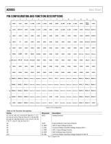
Data Sheet PIN CONFIGURATION AND FUNCTION DESCRIPTIONS 1 IBIAS_ TEST Mnemonic AVSS Description Analog Ground. CLKP D_VINP C_CML C_VINP B_VINP B_CML External Master Clock Input Positive. ADC D Input Voltage Positive. Common-Mode Level Bias Voltage Output ADC C. ADC C Input Voltage Positive. ADC B Voltage Input Positive. Common-Mode Level Bias Voltage Output for ADC B. Rev. A | Page 8 of 56
Open the catalog to page 8
Data Sheet Mnemonic A_VINP IBIAS_TEST CLKN REFCLK D_VINN D_CML C_VINN B_VINN A_CML A_VINN IOUTA_N IOUTA_P AVDD33 LDO15 CP IOUTB_N IOUTB_P AVDD Description ADC A Voltage Input Positive. Test. Connect to ground. External Master Clock Input Negative On-Chip PLL Synthesizer Reference Clock Input. ADC D Input Voltage Negative. Common-Mode Level Bias Voltage Output ADC D. ADC C Input Voltage Negative. ADC B Voltage Input Negative. Common-Mode Level Bias Voltage Output for ADC A. ADC A Voltage Input Negative. DAC A Output Current Negative. DAC A Output Current Positive. 3.3 V Analog Power Supply. On-Chip...
Open the catalog to page 9
Description DAC B Data Input Lane 6 Positive. DAC B Data Input Lane 4 Positive. DAC B Data Input Lane 1 Positive. ADC D Data Output Lane 1 Negative. ADC D Data Output Lane 2 Negative. ADC C Data Output Lane 1 Negative. ADC C Data Output Lane 3 Negative. ADC B Data Output Lane 3 Negative. ADC B Data Output Lane 1 Negative. ADC A Data Output Lane 2 Negative. ADC A Data Output Lane 1 Negative. DAC A Data Input Lane 1 Positive. DAC A Data Input Lane 4 Positive. DAC A Data Input Lane 6 Positive. DAC B Data Input Lane 5 Negative. DAC B Data Input Lane 3 Negative. DAC B Data Input Lane 3 Positive. ADC...
Open the catalog to page 10All Analog Devices catalogs and technical brochures
 HMC722LP3E
8 Pages
 Isolated Sigma-Delta Modulator
17 Pages
 HMC853 Data Sheet
10 Pages
 AN-1084
8 Pages
 AN-1091
2 Pages
 AN_737
8 Pages
 AN-0982
4 Pages
 ADF7024
24 Pages
 AD9915
48 Pages
 AD9914
48 Pages
 ADRF6612
59 Pages
 ADRF6820
48 Pages
 ADL5246
32 Pages
 ADA4961
22 Pages
 AN-1141
8 Pages
 AN-698
36 Pages
 Temperature Sensors
2 Pages
 Reference Circuits
8 Pages
 Precision ADCs
16 Pages
 ADR02ACHIPS: ADR02ACHIPS
8 Pages
 AD9364 RF Agile Transceiver
32 Pages
 Digital Temperature Sensors
2 Pages
 Digital to Analog Converter ICs
12 Pages
 AD1836A: Multichannel 96 kHz Codec
24 Pages


Archived catalogs
 Zero-Drift Amplifiers
2 Pages
 Powering ADI Components
8 Pages


- Ethernet switch
- Industrial network switch
- Acceleration sensor
- Unmanaged switch
- Transceiver module
- Analog Devices motor controller
- Triaxial acceleration sensor
- DC motor controller
- Data acquisition unit
- Analog Devices stepper motor controller
- Industrial converter
- Ethernet transceiver
- Processor
- High-voltage amplifier
- Low-noise amplifier
- Multiplexer
- Compact motor controller
- Gyroscope
- Closed-loop motor controller
- Digital converter