
- Catalogs
- Analog Devices
- AD9914


- Products
- Catalogs
- News & Trends
- Exhibitions
AD9914

AD9914
- 3.5 GSPS internal clock speed with a 12-bit DAC.
- Frequency tuning resolution down to 190 pHz and 16-bit phase tuning resolution.
- Programmable modulus and automatic frequency sweeping capabilities.
- 32-bit parallel datapath interface and 8 frequency/phase offset profiles.
- Phase noise of -128 dBc/Hz at 1 kHz offset at 1396 MHz.
- Wideband SFDR less than -50 dBc.
- Supports both serial and parallel I/O control.
- Operates on 1.8 V/3.3 V power supplies with power-down options.
- DC Specifications: Operates with supply voltages of 1.8 V and 3.3 V, with specific current requirements for different pins. Total power dissipation varies based on operational modes.
- AC Specifications: The REF CLK input frequency ranges from 500 MHz to 3.5 GHz, with specific requirements for duty cycle and input levels. The DAC output frequency range is up to 1750 MHz with specified SFDR values.
Catalog excerpts

3.5 GSPS Direct Digital Synthesizer with 12-Bit DAC AD9914 Data Sheet FEATURES 1.8 V/3.3 V power supplies Software and hardware controlled power-down 88-lead LFCSP package PLL REF CLK multiplier Phase modulation capability Amplitude modulation capability 3.5 GSPS internal clock speed Integrated 12-bit DAC Frequency tuning resolution to 190 pHz 16-bit phase tuning resolution 12-bit amplitude scaling Programmable modulus Automatic linear and nonlinear frequency sweeping capability 32-bit parallel datapath interface 8 frequency/phase offset profiles Phase noise: −128 dBc/Hz (1 kHz offset at 1396 MHz) Wideband SFDR < −50 dBc Serial or parallel I/O control APPLICATIONS Agile LO frequency synthesis Programmable clock generator FM chirp source for radar and scanning systems Test and measurement equipment Acousto-optic device drivers Polar modulator Fast frequency hopping FUNCTIONAL BLOCK DIAGRAM AD9914 HIGH SPEED PARALLEL MODULATION PORT SERIAL OR PARALLEL DATA PORT LINEAR SWEEP BLOCK Document Feedback Information furnished by Analog Devices is believed to be accurate and reliable. However, no responsibility is assumed by Analog Devices for its use, nor for any infringements of patents or other rights of third parties that may result from its use. Specifications subject to change without notice. No license is granted by implication or otherwise under any patent or patent rights of Analog Devices. Trademarks and registered trademarks are the property of their respective owners. One Technology Way, P.O. Box 9106, Norwood, MA 02062-9106, U.S.A. Tel: 781.329.4700 ©2012–2014 Analog Devices, Inc. All rights reserved. Technical Support www.analog.com
Open the catalog to page 1
Data Sheet
Open the catalog to page 2
Data Sheet GENERAL DESCRIPTION AD9914 via a serial or parallel I/O port. The AD9914 also supports a user defined linear sweep mode of operation for generating linear swept waveforms of frequency, phase, or amplitude. A high speed, 32-bit parallel data input port is included, enabling high data rates for polar modulation schemes and fast reprogramming of the phase, frequency, and amplitude tuning words. The AD9914 is a direct digital synthesizer (DDS) featuring a 12-bit DAC. The AD9914 uses advanced DDS technology, coupled with an internal high speed, high performance DAC to form a digitally programmable,...
Open the catalog to page 3
Data Sheet SPECIFICATIONS DC SPECIFICATIONS AVDD (1.8V) and DVDD (1.8V) = 1.8 V ± 5%, AVDD (3.3V) and DVDD_I/O (3.3V) = 3.3 V ± 5%, TA = 25°C, RSET = 3.3 kΩ, IOUT = 20 mA, external reference clock frequency = 3.5 GHz with reference clock (REF CLK) multiplier bypassed, unless otherwise noted. Table 1. Parameter Test Conditions/Comments SUPPLY VOLTAGE DVDD_I/O DVDD AVDD (3.3V) Pin 16, Pin 83 Pin 6, Pin 23, Pin 73 Pin 34, Pin 36, Pin 39, Pin 40, Pin 43, Pin 47, Pin 50, Pin 52, Pin 53, Pin 60 Pin 32, Pin 56, Pin 57 See also the total power dissipation specifications Pin 16, Pin 83 Pin 6, Pin 23,...
Open the catalog to page 4
Data Sheet AC SPECIFICATIONS AVDD (1.8V) and DVDD (1.8V) = 1.8 V ± 5%, AVDD3 (3.3V) and DVDD_I/O (3.3V) = 3.3 V ± 5%, TA = 25°C, RSET = 3.3 kΩ, IOUT = 20 mA, external reference clock frequency = 3.5 GHz with reference clock (REF CLK) multiplier bypassed, unless otherwise noted. Table 2. Parameter REF CLK INPUT REF CLK Multiplier Bypassed Input Frequency Range Duty Cycle Minimum Differential Input Level System Clock (SYSCLK) PLL Enabled VCO Frequency Range VCO Gain (KV) Maximum PFD Rate CLOCK DRIVERS SYNC_CLK Output Driver Frequency Range Duty Cycle Rise Time/Fall Time (20% to 80%) SYNC_OUT Output...
Open the catalog to page 5
AD9914 Parameter PARALLEL PORT TIMING Write Timing Address Setup Time to WR Active Address Hold Time to WR Inactive Data Setup Time to WR Inactive Test Conditions/Comments Data Hold Time to WR Inactive WR Minimum Low Time WR Minimum High Time Minimum WR Time Read Timing Address to Data Valid Address Hold to RD Inactive RD Active to Data Valid RD Inactive to Data Tristate RD Minimum Low Time RD Minimum High Time SERIAL PORT TIMING SCLK Clock Rate (1/tCLK ) SCLK Pulse Width High, tHIGH SCLK Pulse Width Low, tLOW SDIO to SCLK Setup Time, tDS SDIO to SCLK Hold Time, tDH SCLK Falling Edge to Valid...
Open the catalog to page 6
Data Sheet Parameter DATA LATENCY (PIPELINE DELAY) Single Tone Mode or Profile Mode (Matched Latency Disabled) Frequency Phase Amplitude Single Tone Mode or Profile Mode (Matched Latency Enabled) Frequency Phase Amplitude Modulation Mode with 32-Bit Parallel Port (Matched Latency Disabled) Frequency Phase Amplitude Modulation Mode with 32-Bit Parallel Port (Matched Latency Enabled) Frequency Phase Amplitude Sweep Mode (Match Latency Disabled) Frequency Phase Amplitude Sweep Mode (Match Latency Enabled) Frequency Phase Amplitude Test Conditions/Comments SYSCLK cycles = fS = system clock frequency...
Open the catalog to page 7
Data Sheet ABSOLUTE MAXIMUM RATINGS AVDD (1.8 V), DVDD (1.8 V) Supplies AVDD (3.3 V), DVDDJ/O (3.3 V) Supplies Digital InputVoltage Digital Output Current Storage Temperature Range Operating Temperature Range Maximum Junction Temperature Lead Temperature (10 sec Soldering) Stresses above those listed under Absolute Maximum Ratings may cause permanent damage to the device. This is a stress rating only; functional operation of the device at these or any other conditions above those indicated in the operational section of this specification is not implied. Exposure to absolute maximum rating conditions...
Open the catalog to page 8
Data Sheet PIN CONFIGURATION AND FUNCTION DESCRIPTIONS OSK DROVER DRHOLD DRCTL SYNC_IN SYNC_OUT AVDD (3.3V) REF LOOP_FILTER AVDD (1.8V) AVDD (1.8V) REF CLK REF CLK AVDD (3.3V) AVDD (3.3V) AGND AVDD (3.3V) AGND DAC_RSET AVDD (3.3V) AGND DAC_BP NOTES 1. THE EPAD MUST BE SOLDERED TO GROUND. DVDD (1.8V) DGND PS0 PS1 PS2 F0 F1 F2 F3 AVDD (1.8V) AGND AVDD (3.3V) AGND AVDD (3.3V) AGND AGND AVDD (3.3V) AVDD (3.3V) AOUT AOUT AVDD (3.3V) AGND Description Parallel Port Pins. The 32-bit parallel port offers the option for serial or parallel programming of the internal registers. In addition, the parallel...
Open the catalog to page 9
Data Sheet DVDD (1.8V) DGND DVDD_I/O (3.3V) AVDD (1.8V) AGND Description Parallel Port Pin/Address Line. The state of the F0 to F3 function pins determines if this pin acts as a line for direct FSK, PSK, or ASK data or as an address line for programming the internal registers. Parallel Port Pin/Serial Port Synchronization Pin. This pin is D4 for direct FSK, PSK, or ASK data. If serial mode is invoked via F0 to F3, this pin is used to reset the serial port. Parallel Port Pin/Serial Data Output. This pin is D3 for direct FSK, PSK, or ASK data. If serial mode is invoked via F0 to F3, this pin is...
Open the catalog to page 10All Analog Devices catalogs and technical brochures
 HMC722LP3E
8 Pages
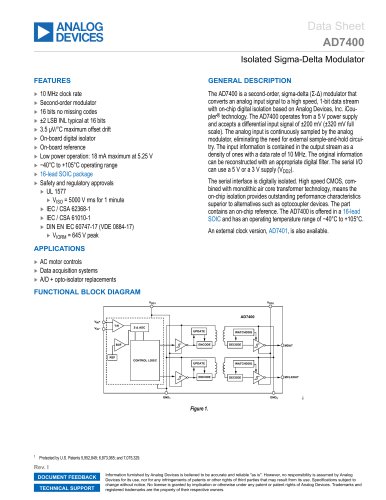 Isolated Sigma-Delta Modulator
17 Pages
 HMC853 Data Sheet
10 Pages
 AN-1084
8 Pages
 AN-1091
2 Pages
 AN_737
8 Pages
 AN-0982
4 Pages
 ADF7024
24 Pages
 AD9915
48 Pages
 ADRF6612
59 Pages
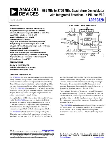 ADRF6820
48 Pages
 ADL5246
32 Pages
 ADA4961
22 Pages
 AN-1141
8 Pages
 AN-698
36 Pages
 Temperature Sensors
2 Pages
 Reference Circuits
8 Pages
 Precision ADCs
16 Pages
 ADR02ACHIPS: ADR02ACHIPS
8 Pages
 AD9364 RF Agile Transceiver
32 Pages
 Digital Temperature Sensors
2 Pages
 Digital to Analog Converter ICs
12 Pages
 AD1836A: Multichannel 96 kHz Codec
24 Pages




























Archived catalogs
 Zero-Drift Amplifiers
2 Pages
 Powering ADI Components
8 Pages




- Ethernet switch
- Industrial network switch
- Acceleration sensor
- Unmanaged switch
- Analog Devices motor controller
- Transceiver module
- Triaxial acceleration sensor
- DC motor controller
- Data acquisition unit
- Analog Devices stepper motor controller
- Industrial converter
- Ethernet transceiver
- Processor
- High-voltage amplifier
- Low-noise amplifier
- Multiplexer
- Compact motor controller
- Digital converter
- Closed-loop motor controller
- Digital motor controller