
- Catalogs
- Analog Devices
- AD9856 CMOS 200 MHz Quadrature Digital Upconverter


- Products
- Catalogs
- News & Trends
- Exhibitions
AD9856 CMOS 200 MHz Quadrature Digital Upconverter
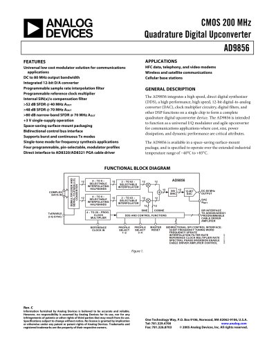
AD9856 CMOS 200 MHz Quadrature Digital Upconverter
- Burst Mode: No external data clock needed; data oversampled using SYSCLK.
- Continuous Mode: Requires full-word input format; TxENABLE acts as a data input clock.
Catalog excerpts

Parameter Temp Test Level Min Typ Max Unit REF CLOCK INPUT CHARACTERISTICS Frequency Range REFCLK Multiplier Disabled Full VI 5 200 > 1 MHz REFCLK Multiplier Enabled at 4 ח Full VI 5 50 MHz REFCLK Multiplier Enabled at 20 Full VI 5 10 MHz Duty Cycle 25װC V 50 % Input Capacitance 25C V 3 pF Input Impedance 25аC V 100 MΩ DAC OUTPUT CHARACTERISTICS Resolution 12 Bits Full-Scale Output Current 5 10 20 mA Gain Error 25C I ТȒ10 +10 %FS Output Offset 25C I 10 е A Differential Nonlinearity 25C V 0.5 LSB Integral Nonlinearity 25аC V 1 LSB Output Capacitance 25C V 5 pF Phase Noise @ 1 kHz Offset, 40 MHz...
Open the catalog to page 3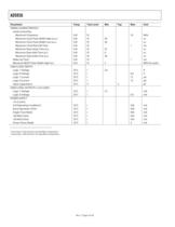
Parameter Temp Test Level Min Typ Max Unit TIMING CHARACTERISTICS Serial Control Bus Maximum Frequency Full IV 10 MHz Minimum Clock Pulse Width High (t > PWH ) Full IV 30 ns Minimum Clock Pulse Width Low (t > PWL ) Full IV 30 ns Maximum Clock Rise/Fall Time Full IV 1 ms Minimum Data Setup Time (t > DS ) Full IV 25 ns Minimum Data Hold Time (t > DH ) Full IV 0 ns Maximum Data Valid Time (t > DV ) Full IV 30 ns Wake-Up Time > 2 Full IV 1 ms Minimum RESET Pulse Width High (t > RH ) Full IV 5 REFCLK cycles CMOS LOGIC INPUTS Logic 1 Voltage 25C I 2.6 V Logic 0 Voltage 25аC I 0.4 V Logic 1 Current...
Open the catalog to page 4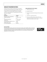
Parameter Rating Maximum Junction Temperature 150аC Storage Temperature −65C to +150аC V > S 4 V Operating Temperature −40C to +85аC Digital Inputs −0.7 V to +V > s Lead Temperature (Soldering 10 sec) 300C Digital Output Current 5 mA Ў > JA Thermal Impedance 38ذC/W > ESD (electrostatic discharge) sensitive device. Electrostatic charges as high as 4000 V readily accumulate on the human body and test equipment and can discharge without detection. Although this product features proprietary ESD protection circuitry, permanent damage may occur on devices subjected to high energy electrostatic discharges....
Open the catalog to page 5
Functional Block Mode Description Operating Modes 1. Complex quadrature modulator mode. 2. Single-tone output mode. Input Data Format Programmable: 12-bit, 6-bit, or 3-bit input formats. Data input to the AD9856 is 12-bit, twos complement. Complex I/Q symbol component data is required to be at least 2 oversampled, depending upon configuration. Input Sample Rate Up to 50 Msamples/sec @ 200 MHz SYSCLK rate. Input Reference Clock Frequency For DC to 80 MHz A > OUT operation (200 MHz SYSCLK rate) with REFCLK multiplier enabled: 10 MHz to50 MHz, programmable via control bus; with REFCLK multiplier...
Open the catalog to page 7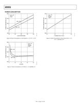
S = +3VCIC = 2+25C +V > S = +3VCIC = 2200 MHz +25аC HB3 = OFFHB3 = ON +V > POWER CONSUMPTION (mW) POWER CONSUMPTION (mW) 800100012001400 1600 CLOCK SPEED (MHz) 10501150 125013501450 Tx ENABLE DUTY CYCLE 140120160180200 257550100 > 00637-C-020 S = +3VCIC = 2200 MHz+25C 64 HB3 = OFFHB3 = ON +V > POWER CONSUMPTION (mW) 12001300 140015001600 CIC RATE 1603248 > 00637-C-021
Open the catalog to page 12
Register AD9856 Register Layout Address (hex) Bit 7 Bit 6 Bit 5 Bit 4 Bit 3 Bit 2 Bit 1 Bit 0 Default (hex) Profile 00 SDO Active LSB First REFCLK Mult.<4> REFCLK Mult.<3> REFCLK Mult.<2> REFCLK Mult.<1> REFCLK Mult.<0> Reserved 15 N/A 01 CIC Gain Continuous Mode Full Sleep Mode Single-tone Mode Bypass Inverse Sinc Filter Bypass REFCLK Mult. Input Format Select <1> Input Format Select <0> 06 N/A 02 Frequency Tuning Word <7:0> 04 1 03 Frequency Tuning Word <15:8> 00 1 04 Frequency Tuning Word <23:16> 00 1 05 Frequency Tuning Word <31:24> 00 1 06 Interpolator Rate <5> Interpolator Rate <4> Interpolator...
Open the catalog to page 13
Input Format Select Register Address 01h, Bits 1 and 0, form the input format mode bits. 10b = 12-bit mode 01b = 6-bit mode 00b = 3-bit mode Default value is 10b (12-bit mode). > SDO Active Register Address 00h, Bit 7. Active high indicates serial port uses dedicated in/out lines. Default low configures serial port as single-line I/O. LSB Firstח Register Address 00h, Bit 6. Active high indicates serial port access is LSB-to-MSB format. Default low indicates MSB-to-LSB format. > REFCLK Multiplierח Register Address 00h, Bits 5, 4, 3, 2, 1 form the reference clock multiplier. Valid entries range...
Open the catalog to page 14
The sampled carrier is ultimately destined to serve as the input data to the digital-to-analog converter (DAC) integrated on the AD9856. The DAC output spectrum is distorted due to the intrinsic zero-order hold effect associated with DAC-generated signals. This distortion is deterministic, however, and follows the familiar SIN(x)/x (or SINC) envelope. Because the SINC distortion is predictable, it is also correctabletherefore, the presence of the optional inverse SINC filter preceding the DAC. This is a FIR filter, which has a transfer function conforming to the inverse of the SINC response....
Open the catalog to page 16
For continuous-mode input timing, the TxENABLE pin can be thought of as a data input clock running at half the input sample rate (f > W /2). In addition to synchronization, for contin-uous mode timing, the TxENABLE input indicates whether an I or Q input is being presented to the D<11:0> pins. It is intended that data is presented in alternating fashion such that I data is followed by Q data. Stated another way, the TxENABLE pin should maintain approximately a 50/50 duty cycle. As in burst mode, the rising edge of TxENABLE synchronizes the AD9856 to the input data rate and the data is registered...
Open the catalog to page 17
load that the AD9856 sees for signals within the filter pass band. For example, a 50 Ω terminated input/output low-pass filter looks like a 25 Ω load to the AD9856. The output compliance voltage of the AD9856 is −0.5 V to +1.5 V. Any signal developed at the DAC output should not exceed +1.5 V, otherwise, signal distortion results. Furthermore, the signal may extend below ground as much as 0.5 V without damage or signal distortion. The use of a transformer with a grounded center tap for common-mode rejection results in signals at the AD9856 DAC output pins that are symmetrical about ground. As...
Open the catalog to page 26
INSTRUCTION CYCLEDATA TRANSFER CYCLESCLKCSI SDIO I > 7 6 I > 5 I > 4 I > 3 I > 2 I > 1 I > D > 7 D > 6 D > 5 D > 4 D > 3 D > 2 D > 1 D > > 00637-C-044 INSTRUCTION CYCLEDATA TRANSFER CYCLESCL CSI K SDIO I > 7 6 I > 5 I > 4 I > 3 I > 2 I > 1 I > D > O7 D > O6 D > O5 D > O4 D > O3 D > O2 D > O1 D > O0 00637-C-047
Open the catalog to page 27All Analog Devices catalogs and technical brochures
 HMC722LP3E
8 Pages
 Isolated Sigma-Delta Modulator
17 Pages
 HMC853 Data Sheet
10 Pages
 AN-1084
8 Pages
 AN-1091
2 Pages
 AN_737
8 Pages
 AN-0982
4 Pages
 ADF7024
24 Pages
 AD9915
48 Pages
 AD9914
48 Pages
 ADRF6612
59 Pages
 ADRF6820
48 Pages
 ADL5246
32 Pages
 ADA4961
22 Pages
 AN-1141
8 Pages
 AN-698
36 Pages
 Temperature Sensors
2 Pages
 Reference Circuits
8 Pages
 Precision ADCs
16 Pages
 ADR02ACHIPS: ADR02ACHIPS
8 Pages
 AD9364 RF Agile Transceiver
32 Pages
 Digital Temperature Sensors
2 Pages
 Digital to Analog Converter ICs
12 Pages
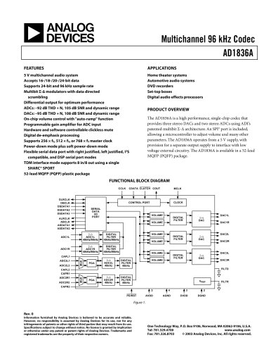 AD1836A: Multichannel 96 kHz Codec
24 Pages




























Archived catalogs
 Zero-Drift Amplifiers
2 Pages
 Powering ADI Components
8 Pages




- Ethernet switch
- Industrial network switch
- Acceleration sensor
- Unmanaged switch
- Analog Devices motor controller
- Transceiver module
- Triaxial acceleration sensor
- DC motor controller
- Data acquisition unit
- Analog Devices stepper motor controller
- Industrial converter
- Ethernet transceiver
- Processor
- High-voltage amplifier
- Low-noise amplifier
- Multiplexer
- Compact motor controller
- Digital converter
- Closed-loop motor controller
- Digital motor controller