- Catalogs
- Analog Devices
- AD9680: 14-Bit, 1 GSPS JESD204B, Dual Analog-to-Digital Converter
AD9680: 14-Bit, 1 GSPS JESD204B, Dual Analog-to-Digital Converter
1 /64Pages

AD9680: 14-Bit, 1 GSPS JESD204B, Dual Analog-to-Digital Converter
1 /64Pages
Catalog excerpts
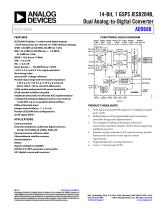
14-Bit, 1 GSPS JESD204B, Dual Analog-to-Digital Converter AD9680 Data Sheet FEATURES VIN+B VIN–B CONTROL REGISTERS FAST DETECT CLOCK GENERATION DRGND DGND SDIO SCLK CSB PDWN/ STBY APPLICATIONS Communications Diversity multiband, multimode digital receivers 3G/4G, TD-SCDMA, W-CDMA, GSM, LTE General-purpose software radios Ultrawideband satellite receivers Instrumentation Radars Signals intelligence (SIGINT) DOCSIS 3.0 CMTS upstream receive paths HFC digital reverse path receivers JESD204B HIGH SPEED SERIALIZER + Tx OUTPUTS BUFFER VIN+A VIN–A FAST DETECT JESD204B (Subclass 1) coded serial digital outputs 1.65 W total power per channel at 1 GSPS (default settings) SFDR = 85 dBFS at 340 MHz, 80 dBFS at 1 GHz SNR = 65.3 dBFS at 340 MHz (AIN = −1.0 dBFS), 61.4 dBFS at 1 GHz ENOB = 10.8 bits at 10 MHz DNL = ±0.5 LSB INL = ±2.5 LSB Noise density = −154 dBFS/Hz at 1 GSPS 1.25 V, 2.5 V, and 3.3 V dc supply operation No missing codes Internal ADC voltage reference Flexible input range and termination impedance 1.46 V p-p to 1.94 V p-p (1.70 V p-p nominal) 400 Ω, 200 Ω, 100 Ω, and 50 Ω differential 2 GHz usable analog input full power bandwidth 95 dB channel isolation/crosstalk Amplitude detect bits for efficient AGC implementation 2 integrated wideband digital processors per channel 12-bit NCO, up to 4 cascaded half-band filters Differential clock input Integer clock divide by −1, 2, 4, or 8 Flexible JESD204B lane configurations Small signal dither Wide full power bandwidth supports IF sampling of signals up to 2 GHz. Buffered inputs with programmable input termination eases filter design and implementation. Four integrated wideband decimation filters and numerically controlled oscillator (NCO) blocks supporting multiband receivers. Flexible serial port interface (SPI) controls various product features and functions to meet specific system requirements. Programmable fast overrange detection. 9 mm × 9 mm 64-lead LFCSP. Document Feedback Information furnished by Analog Devices is believed to be accurate and reliable. However, no responsibility is assumed by Analog Devices for its use, nor for any infringements of patents or other rights of third parties that may result from its use. Specifications subject to change without notice. No license is granted by implication or otherwise under any patent or patent rights of Analog Devices. Trademarks and registered trademarks are the property of their respective owners. One Technology Way, P.O. Box 9106, Norwood, MA 02062-9106, U.S.A. Tel: 781.329.4700 ©2014 Analog Devices, Inc. All rights reserved. Technical Support www.analog.com
Open the catalog to page 1
Data Sheet REVISION HISTORY 5/14—Revision 0: Initial Version
Open the catalog to page 2
Data Sheet GENERAL DESCRIPTION The AD9680 is a dual, 14-bit, 1 GSPS analog-to-digital converter (ADC). The device has an on-chip buffer and sampleand-hold circuit designed for low power, small size, and ease of use. This device is designed for sampling wide bandwidth analog signals of up to 2 GHz. The AD9680 is optimized for wide input bandwidth, high sampling rate, excellent linearity, and low power in a small package. The dual ADC cores feature a multistage, differential pipelined architecture with integrated output error correction logic. Each ADC features wide bandwidth inputs supporting...
Open the catalog to page 3
Data Sheet SPECIFICATIONS DC SPECIFICATIONS AVDD1 = 1.25 V, AVDD2 = 2.5 V, AVDD3 = 3.3 V, AVDD1_SR = 1.25 V, DVDD = 1.25 V, DRVDD = 1.25 V, SPIVDD = 1.8 V, specified maximum sampling rate (1000 MSPS), 1.7 V p-p full-scale differential input, 1.0 V internal reference, AIN = −1.0 dBFS, default SPI settings, TA = 25°C, unless otherwise noted. Table 1. Parameter RESOLUTION ACCURACY No Missing Codes Offset Error Offset Matching Gain Error Gain Matching Differential Nonlinearity (DNL) Integral Non-Linearity (INL) TEMPERATURE DRIFT Offset Error Gain Error INTERNAL VOLTAGE REFERENCE Voltage INPUT-REFERRED...
Open the catalog to page 4
Data Sheet AC SPECIFICATIONS AVDD1 = 1.25 V, AVDD2 = 2.5 V, AVDD3 = 3.3 V, AVDD1_SR = 1.25 V, DVDD = 1.25 V, DRVDD = 1.25 V, SPIVDD = 1.8 V, specified maximum sampling rate, 1.7 V p-p full-scale differential input, 1.0 V internal reference, AIN = −1.0 dBFS, default SPI settings, TA = 25°C, unless otherwise noted. Table 2. Parameter 1 ANALOG INPUT FULL SCALE NOISE DENSITY 2 SIGNAL-TO-NOISE RATIO (SNR) 3 fIN = 10 MHz fIN = 170 MHz fIN = 340 MHz fIN = 450 MHz fIN = 765 MHz fIN = 985 MHz fIN = 1950 MHz SNR AND DISTORTION RATIO (SINAD)3 fIN = 10 MHz fIN = 170 MHz fIN = 340 MHz fIN = 450 MHz fIN =...
Open the catalog to page 5
Data Sheet Parameter 1 fIN = 765 MHz fIN = 985 MHz fIN = 1950 MHz TWO-TONE INTERMODULATION DISTORTION (IMD), AIN1 AND AIN2 = −7 dBFS fIN1 = 185 MHz, fIN2 = 188 MHz fIN1 = 338 MHz, fIN2 = 341 MHz CROSSTALK 4 FULL POWER BANDWIDTH 5 Unit dBFS dBFS dBFS dBFS dBFS dB GHz See the AN-835 Application Note, Understanding High Speed ADC Testing and Evaluation, for definitions and for details on how these tests were completed. Noise density is measured at a low analog input frequency (30 MHz). 3 See Table 9 for recommended settings for full scale voltage and buffer current setting 4 Crosstalk is measured...
Open the catalog to page 6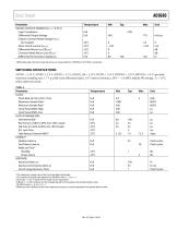
Data Sheet Parameter DIGITAL OUTPUTS (SERDOUTx±, x = 0 TO 3) Logic Compliance Differential Output Voltage Output Common-Mode Voltage (VCM) AC Coupled Short-Circuit Current (IDshort) Differential Return Loss (RLDIFF) 1 Common-Mode Return Loss (RLCM) 1 Differential Termination Impedance 1 Differential and common-mode return loss is measured from 100 MHz to 0.75 MHz × baud rate. SWITCHING SPECIFICATIONS AVDD1 = 1.25 V, AVDD2 = 2.5 V, AVDD3 = 3.3 V, AVDD1_SR = 1.25 V, DVDD = 1.25 V, DRVDD = 1.25 V, SPIVDD = 1.8 V, specified maximum sampling rate, 1.7 V p-p full-scale differential input, 1.0 V internal...
Open the catalog to page 7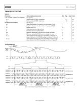
Data Sheet TIMING SPECIFICATIONS Table 5. Parameter CLK+ to SYSREF+ TIMING REQUIREMENTS tSU_SR tH_SR SPI TIMING REQUIREMENTS tDS tDH tCLK tS tH tHIGH tLOW tEN_SDIO Test Conditions/Comments See Figure 3 Device clock to SYSREF+ setup time Device clock to SYSREF+ hold time See Figure 4 Setup time between the data and the rising edge of SCLK Hold time between the data and the rising edge of SCLK Period of the SCLK Setup time between CSB and SCLK Hold time between CSB and SCLK Minimum period that SCLK must be in a logic high state Minimum period that SCLK must be in a logic low state Time required...
Open the catalog to page 8All Analog Devices catalogs and technical brochures
 HMC722LP3E
8 Pages
 Isolated Sigma-Delta Modulator
17 Pages
 HMC853 Data Sheet
10 Pages
 AN-1084
8 Pages
 AN-1091
2 Pages
 AN_737
8 Pages
 AN-0982
4 Pages
 ADF7024
24 Pages
 AD9915
48 Pages
 AD9914
48 Pages
 ADRF6612
59 Pages
 ADRF6820
48 Pages
 ADL5246
32 Pages
 ADA4961
22 Pages
 AN-1141
8 Pages
 AN-698
36 Pages
 Temperature Sensors
2 Pages
 Reference Circuits
8 Pages
 Precision ADCs
16 Pages
 ADR02ACHIPS: ADR02ACHIPS
8 Pages
 AD9364 RF Agile Transceiver
32 Pages
 Digital Temperature Sensors
2 Pages
 Digital to Analog Converter ICs
12 Pages
 AD1836A: Multichannel 96 kHz Codec
24 Pages


Archived catalogs
 Zero-Drift Amplifiers
2 Pages
 Powering ADI Components
8 Pages


- Ethernet switch
- Industrial network switch
- Acceleration sensor
- Unmanaged switch
- Transceiver module
- Analog Devices motor controller
- Triaxial acceleration sensor
- DC motor controller
- Data acquisition unit
- Analog Devices stepper motor controller
- Industrial converter
- Ethernet transceiver
- High-voltage amplifier
- Low-noise amplifier
- Multiplexer
- Compact motor controller
- Gyroscope
- Closed-loop motor controller