
- Catalogs
- Analog Devices
- AD9625: 12-Bit 2.0 GSPS, 1.3 V/2.5 V Analog-to-Digital Converted


- Products
- Catalogs
- News & Trends
- Exhibitions
AD9625: 12-Bit 2.0 GSPS, 1.3 V/2.5 V Analog-to-Digital Converted

AD9625: 12-Bit 2.0 GSPS, 1.3 V/2.5 V Analog-to-Digital Converted
- 12-bit resolution with no missing codes.
- Sampling rate of 2.0 GSPS.
- Signal-to-Noise Ratio (SNR) of 59 dBFS for input frequencies up to 1 GHz.
- Spurious-Free Dynamic Range (SFDR) of 80 dBc for input frequencies up to 1 GHz.
- Power consumption of 3.5 W at 2.0 GSPS.
- Supports differential analog and clock inputs.
- High-speed JESD204B serial output with flexible lane configurations.
- Built-in digital test patterns and selectable digital output modes.
- DC Specifications: Offset error of ±0.5 LSB, gain error of ±8% FSR, differential input voltage range of 1.1 V p-p.
- AC Specifications: Noise floor of -149.5 dBFS/Hz, effective number of bits (ENOB) of 9.4 bits at 100 MHz input frequency.
- Digital Specifications: Supports differential input voltages for clock and SYSREF inputs, with logic compliance for CMOS and LVDS.
- Switching Specifications: Maximum clock rate of 2000 MSPS, with a clock pulse width duty cycle of 50% ± 5%.
- FFT Plots: Demonstrates performance at 2.0 GSPS with various input frequencies, highlighting SFDR and SNR values.
- SNR/SFDR vs. Amplitude: Shows the relationship between signal amplitude and performance metrics.
- Current and Power vs. Sample Rate: Illustrates power consumption across different sample rates.
- ADC Architecture: Utilizes a pipelined structure with flash ADCs and MDACs for efficient sampling and error correction.
- Fast Detect: Provides rapid detection of input signal levels to prevent ADC overload.
- Gain Threshold Operation: Uses thresholds to manage calibration updates based on signal amplitude.
- Architecture: Features two DDCs with independent frequency synthesizers and mixers, supporting high and low bandwidth modes.
- Decimation and Filtering: Employs decimate-by-8 polyphase filters for efficient bandwidth management and noise reduction.
Catalog excerpts
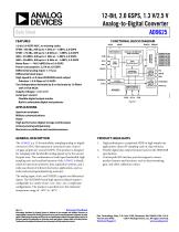
Data Sheet FUNCTIONAL BLOCK DIAGRAM AVDD DRVDD DRGND DIGITAL INTERFACE AND CONTROL RBIAS CONTROL REGISTERS SYSREF± CLK± CLOCK MANAGEMENT CMOS DIGITAL INPUT/OUTPUT CMOS DIGITAL INPUT/ OUTPUT LVDS DIGITAL INPUT/ OUTPUT 12-bit 2.0 GSPS ADC, no missing codes SFDR = 80 dBc, AIN up to 1 GHz at −1 dBFS, 2.0 GSPS SFDR = 76 dBc, AIN up to 1.8 GHz at −1 dBFS, 2.0 GSPS SNR = 59 dBFS, AIN up to 1 GHz at −1 dBFS, 2.0 GSPS SNR = 58 dBFS, AIN up to 1.8 GHz at −1 dBFS, 2.0 GSPS Noise floor = −149.5 dBFS/Hz at 2.0 GSPS Power consumption: 3.5 W at 2.0 GSPS Differential analog input: 1.1 V p-p Differential clock input High speed 6- or 8-lane JESD204B serial output Subclass 1: 5.0 Gbps at 2.0 GSPS Two independent decimate by 8 or decimate by 16 filters with 10-bit NCOs Supply voltages: 1.3 V, 2.5 V Serial port control Flexible digital output modes Built-in selectable digital test patterns APPLICATIONS Spectrum analyzers Military communications Radar High performance digital storage oscilloscopes Active jamming/antijamming Electronic surveillance and countermeasures GENERAL DESCRIPTION PRODUCT HIGHLIGHTS The AD9625 is a 12-bit monolithic sampling analog-to-digital converter (ADC) that operates at conversion rates of up to 2.0 giga samples per second (GSPS). This product is designed for sampling wide bandwidth analog signals up to the second Nyquist zone. The combination of wide input bandwidth, high sampling rate, and excellent linearity of the AD9625 is ideally suited for spectrum analyzers, data acquisition systems, and a wide assortment of military electronics applications, such as radar and jamming/antijamming measures. High performance: exceptional SFDR in high sample rate applications, direct RF sampling, and on-chip reference. Flexible digital data output formats based on the JESD204B specification. Control path SPI interface port that supports various product features and functions, such as data formatting, gain, and offset calibration values. The analog input, clock, and SYSREF± signals are differential inputs. The JESD204B-based high speed serialized output is configurable in a variety of one-, two-, four-, six-, or eight-lane configurations. The product is specified over the industrial temperature range of −40°C to +85°C. Document Feedback Information furnished by Analog Devices is believed to be accurate and reliable. However, no responsibility is assumed by Analog Devices for its use, nor for any infringements of patents or other rights of third parties that may result from its use. Specifications subject to change without notice. No license is granted by implication or otherwise under any patent or patent rights of Analog Devices. Trademarks and registered trademarks are the property of their respective owners. One Technology Way, P.O. Box 9106, Norwood, MA 02062-9106, U.S.A. Tel: 781.329.4700 ©2014 Analog Devices, Inc. All rights reserved. Technical Support
Open the catalog to page 1
Data Sheet REVISION HISTORY 5/14—Revision 0: Initial Version
Open the catalog to page 2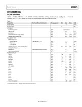
Data Sheet SPECIFICATIONS DC SPECIFICATIONS AVDD1 = DVDD1 = DRVDD1 = 1.3 V, AVDD2 = DVDD2 = DRVDD2 = 2.5 V, specified maximum sampling rate, 1.2 V internal reference, AIN = −1.0 dBFS, default SPI settings, dc-coupled output data, unless otherwise noted. Table 1. Parameter SPEED GRADE RESOLUTION ACCURACY No Missing Codes Offset Error Gain Error Differential Nonlinearity (DNL) Integral Nonlinearity (INL) ANALOG INPUTS Differential Input Voltage Range Resistance Capacitance Internal Common-Mode Voltage (VCM) Analog Full Power Bandwidth Input Referred Noise POWER SUPPLIES AVDD1 AVDD2 DRVDD1 DRVDD2...
Open the catalog to page 3
Data Sheet AC SPECIFICATIONS AVDD1 = DVDD1 = DRVDD1 = 1.3 V, AVDD2 = DVDD2 = DRVDD2 = 2.5 V, specified maximum sampling, 1.2 V internal reference, AIN = −1.0 dBFS, sample clock input = 1.65 V p-p differential, default SPI settings, unless otherwise noted. Table 2. Parameter SPEED GRADE ANALOG INPUT NOISE DENSITY SIGNAL-TO-NOISE RATIO (SNR) fIN = 100 MHz fIN = 500 MHz fIN = 1000 MHz fIN = 1800 MHz SIGNAL-TO-NOISE AND DISTORTION (SINAD) fIN = 100 MHz fIN = 500 MHz fIN = 1000 MHz fIN = 1800 MHz EFFECTIVE NUMBER OF BITS (ENOB) fIN = 100 MHz fIN = 500 MHz fIN = 1000 MHz fIN = 1800 MHz SPURIOUS FREE...
Open the catalog to page 4
Data Sheet Parameter Input Resistance (Differential) Input Capacitance LOGIC INPUTS (SDIO, SCLK, CSB) Logic Compliance Voltage Logic 1 Logic 0 Input Resistance Input Capacitance SYNCB+/SYNCB− INPUT (SYNCINB+, SYNCINB−) Logic Compliance Input Voltage Differential Common Mode Input Resistance (Differential) Input Capacitance LOGIC OUTPUT (SDIO) Logic Compliance Voltage Logic 1 (IOH = 800 μA) Logic 0 (IOL = 50 μA) DIGITAL OUTPUTS (SERDOUT[x]±) Compliance Output Voltage Differential Offset Differential Return Loss (RLDIFF) 1 Common-Mode Return Loss (RLCM)1 Differential Termination Impedance RESET...
Open the catalog to page 5
Data Sheet SWITCHING SPECIFICATIONS AVDD1 = DVDD1 = DRVDD1 = 1.3 V, AVDD2 = DVDD2 = DRVDD2 = 2.5 V, specified maximum sampling rate, 1.2 V internal reference, AIN = −1.0 dBFS, default SPI settings, unless otherwise noted. Table 4. Parameter CLOCK (CLK±) Maximum Clock Rate Minimum Clock Rate Clock Pulse Width High Clock Pulse Width Low SYSREF (SYSREF±) 2 Setup Time (tSU_SR) Hold Time (tH_SR) FAST DETECT OUTPUT (FD) Latency OUTPUT PARAMETERS (SERDOUT[x]±) Rise Time Fall Time Pipeline Latency APERTURE Delay Uncertainty (Jitter) Out-of-Range Recovery Time 1 2 Test Conditions/Comments Full Full Full...
Open the catalog to page 6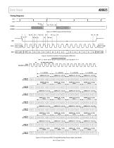
Data Sheet Timing Diagrams CLK– CLK+ SYSREF– SYSREF+ Figure 2. SYSREF± Setup and Hold Timing tDS SDIO DON’T CARE DON’T CARE DON’T CARE Figure 3. Serial Port Interface Timing Diagram (MSB First) JESD204B INTERFACE M = 1; L = 8; N = 12; N' = 16; CF = 0; CS = 0; CS = 0...4; K = 32; HD = 1; F = 1 500ps MIN (2.0GHz) CLK+ (ENCODE CLOCK) SAMPLE N [3:0], CCCC LANE B± @ 5.0Gbps Figure 4. CLK Input and DOUT Timing Relationship (Generic Eight-Lane Mode) Rev. 0 | Page 7 of 56 SAMPLE N + 3 [3:0], CCCC LANE H± @ 5.0Gbps SAMPLE N + 2 [3:0], CCCC LANE F± @ 5.0Gbps SAMPLE N + 1 [3:0], CCCC LANE D± @ 5.0Gbps SCLK...
Open the catalog to page 7All Analog Devices catalogs and technical brochures
 HMC722LP3E
8 Pages
 Isolated Sigma-Delta Modulator
17 Pages
 HMC853 Data Sheet
10 Pages
 AN-1084
8 Pages
 AN-1091
2 Pages
 AN_737
8 Pages
 AN-0982
4 Pages
 ADF7024
24 Pages
 AD9915
48 Pages
 AD9914
48 Pages
 ADRF6612
59 Pages
 ADRF6820
48 Pages
 ADL5246
32 Pages
 ADA4961
22 Pages
 AN-1141
8 Pages
 AN-698
36 Pages
 Temperature Sensors
2 Pages
 Reference Circuits
8 Pages
 Precision ADCs
16 Pages
 ADR02ACHIPS: ADR02ACHIPS
8 Pages
 AD9364 RF Agile Transceiver
32 Pages
 Digital Temperature Sensors
2 Pages
 Digital to Analog Converter ICs
12 Pages
 AD1836A: Multichannel 96 kHz Codec
24 Pages




























Archived catalogs
 Zero-Drift Amplifiers
2 Pages
 Powering ADI Components
8 Pages




- Ethernet switch
- Industrial network switch
- Acceleration sensor
- Unmanaged switch
- Analog Devices motor controller
- Transceiver module
- Triaxial acceleration sensor
- DC motor controller
- Analog Devices stepper motor controller
- Industrial converter
- Ethernet transceiver
- Processor
- High-voltage amplifier
- Low-noise amplifier
- Multiplexer
- Compact motor controller
- Closed-loop motor controller
- Digital motor controller