
- Catalogs
- Analog Devices
- AD9066 Dual, 6-Bit, 60 MSPS Monlithic A/D Converter


- Products
- Catalogs
- News & Trends
- Exhibitions
AD9066 Dual, 6-Bit, 60 MSPS Monlithic A/D Converter
AD9066 Dual, 6-Bit, 60 MSPS Monlithic A/D Converter
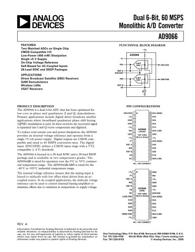
The AD9066 is a dual 6-bit ADC designed for cost-effective I and Q demodulators, mainly in digital direct broadcast satellite systems. It operates on a +5V supply, includes an internal voltage reference, and supports CMOS-compatible outputs with conversion rates up to 60 MSPS.
- Full-scale input range: 500 mV ± 5%
- Power dissipation: 400 mW
- Operating temperature: 0°C to 70°C (commercial), -40°C to +85°C (industrial)
- Package: 28-lead SOIC and SSOP
- Input offset: ±1.0 LSBs
- Input bandwidth: 100 MHz
- Max conversion rate: 60 MSPS
- ENOB: 5.3 to 5.7 bits
- SINAD: 33 to 36 dB
- DBS Receivers
- QAM Demodulators
- Wireless LANs
- VSAT Receivers
The AD9066 has a 28-pin setup with specific pins for analog inputs, voltage references, and digital outputs, including ENCODE for clock input, INA and INB for analog inputs, and REF A and REF B for reference voltages.
Suitable for AC and DC coupled applications, the AD9066 includes internal biasing for AC-coupled inputs and allows external biasing for DC-coupled applications to minimize offsets. Gain adjustments can be made by altering the voltage across its resistor ladders.
Optimal performance is achieved with a single low impedance ground plane, connecting analog and digital grounds at the device. Minimizing the length and load on output data lines is recommended to reduce power supply transients.
Though equipped with proprietary ESD protection, the AD9066 requires proper ESD precautions to prevent performance issues.
Available in various temperature grades and package options, including AD9066AR for industrial and AD9066JR for commercial use.
Catalog excerpts
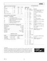
ABSOLUTE MAXIMUM RATINGS PIN DESCRIPTIONS PinMinMaxUnit AR:JRARSPinPin ENCODE0.5+V > S V+V > S 7.0VINA, INB֖0.5+V No.No.NameFunction > S VVT2.5+V 122ENCODETTL Compatible CMOS Clock,Samples on Rising Edge.223+V > S VREF A, REF B0.5+V > S VVB0.0+V > S +5 V Supply for Digital Input.324GNDGround.425GNDGround.526+V > S V D0֖D5 Current OUT20mA > EXPLANATION OF TEST LEVELS S +5 V Supply (Analog).627INAChannel A Analog Input.728GNDGround.81+V Test LevelDescription I100% Production TestedII100% Production Tested at +25 C, andSample Tested at Specified TemperaturesIIISample Tested OnlyIVParameter Is Guaranteed...
Open the catalog to page 3All Analog Devices catalogs and technical brochures
 HMC722LP3E
8 Pages
 Isolated Sigma-Delta Modulator
17 Pages
 HMC853 Data Sheet
10 Pages
 AN-1084
8 Pages
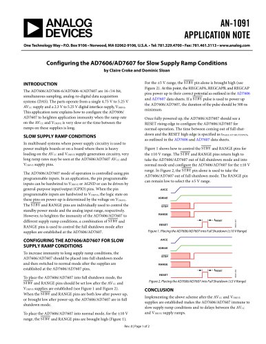 AN-1091
2 Pages
 AN_737
8 Pages
 AN-0982
4 Pages
 ADF7024
24 Pages
 AD9915
48 Pages
 AD9914
48 Pages
 ADRF6612
59 Pages
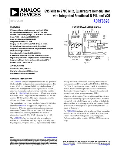 ADRF6820
48 Pages
 ADL5246
32 Pages
 ADA4961
22 Pages
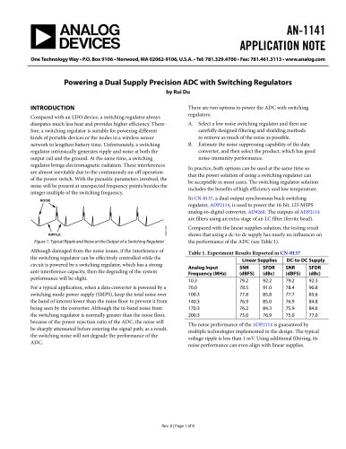 AN-1141
8 Pages
 AN-698
36 Pages
 Temperature Sensors
2 Pages
 Reference Circuits
8 Pages
 Precision ADCs
16 Pages
 ADR02ACHIPS: ADR02ACHIPS
8 Pages
 AD9364 RF Agile Transceiver
32 Pages
 Digital Temperature Sensors
2 Pages
 Digital to Analog Converter ICs
12 Pages
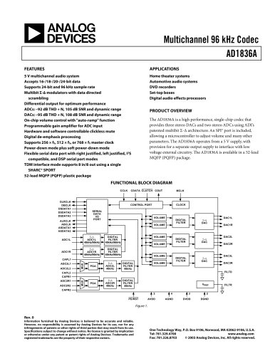 AD1836A: Multichannel 96 kHz Codec
24 Pages




























Archived catalogs
 Zero-Drift Amplifiers
2 Pages
 Powering ADI Components
8 Pages




- Ethernet switch
- Industrial network switch
- Acceleration sensor
- Unmanaged switch
- Analog Devices motor controller
- Transceiver module
- Triaxial acceleration sensor
- DC motor controller
- Data acquisition unit
- Analog Devices stepper motor controller
- Industrial converter
- Ethernet transceiver
- Processor
- High-voltage amplifier
- Low-noise amplifier
- Multiplexer
- Compact motor controller
- Digital converter
- Closed-loop motor controller
- Digital motor controller