
- Catalogs
- Analog Devices
- AD8509 9-Channel, Multiplexed Input, LCD Driver


- Products
- Catalogs
- News & Trends
- Exhibitions
AD8509 9-Channel, Multiplexed Input, LCD Driver
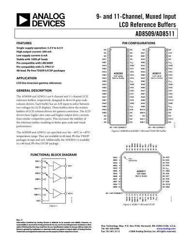
AD8509 9-Channel, Multiplexed Input, LCD Driver
Catalog excerpts
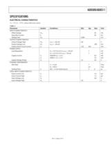
Parameter Symbol Conditions Min Typ Max Unit INPUT CHARACTERISTICS Offset Voltage V > OS 20 mV Input Bias Current I > B 50 nA Voltage Gain A > VO 0.985 V/V OUTPUT CHARACTERISTICS Output Voltage High V > OH I > LOAD = +20 mA 4.8 V Output Voltage Low V > OL I > LOAD = ТȒ20 mA 200 mV Output Short-Circuit Current I > SC 120 350 mA POWER SUPPLY Load Regulation V > IN = 0.5 V to 4.5 V, I > SOURCE = 20 mA 7 mV V > IN = 0.5 V to 4.5 V, I > SINK = 20 mA 7 mV Supply Current I > SY AD8509, V > IN = 2.5 V 8.5 mA I > SY AD8511, V > IN = 2.5 V 10 mA Supply Voltage Range V > S 3.3 6.5 V DYNAMIC PERFORMANCE...
Open the catalog to page 3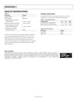
Parameter Rating Supply Voltage 7 V > Input Voltage GND to V > S Storage Temperature Range > TSSOP (RV-48) − 65C to +150аC 48-Lead, Pb-Free SSOP (RV-48) 115 42 C/W Package Type Ў > JA ؎ > JC Unit Operating Temperature Range آȒ 40C to +85аC 48-Lead, Pb-Free LFCSP (CP-48-1) 125 29 C/W Junction Temperature Range TSSOP (RV-48) Package ТȒ 65C to +150аC Lead Temperature Range > (Soldering, 60 sec) 300C A/B Select Input Logic High INAx Logic Low INBx > ESD (electrostatic discharge) sensitive device. Electrostatic charges as high as 4000 V readily accumulate on the human body and test equipment and can...
Open the catalog to page 4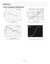
10987654335֖15525456585105 1k1001010.1100101 V > S =5VR V > S =5VT > L =NOLOAD > A =25C SOURCE SINK > SUPPLY CURRENT (mA) OUTPUT VOLTAGE (mV) 03237-003 03237-005 TEMPERATURE(аC) LOADCURRENT(mA) >
Open the catalog to page 6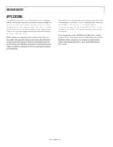
The AD8509 and AD8511 are CMOS buffers with A/B inputs that are used to select between two different reference voltages set up by an external resistor ladder. Input bias currents are orders of magnitude less than competitive parts. This allows very large resistor ladders to be used to save supply current. A guaranteed value of 50 nA is much higher than actual values and is limited by leakage in the test system. Buffer outputs are designed to drive resistive loads. They are also stable with capacitive loads, so no resistors should be used in series with these outputs to attain the best display...
Open the catalog to page 8
AD8509/AD8511 NOTES > 2006 Analog Devices, Inc. All rights reserved. Trademarks and registered trademarks are the property of their respective owners. C03237-0-2/06(C) Rev. C | Page 12 of 12 size="-1">
Open the catalog to page 12All Analog Devices catalogs and technical brochures
 HMC722LP3E
8 Pages
 Isolated Sigma-Delta Modulator
17 Pages
 HMC853 Data Sheet
10 Pages
 AN-1084
8 Pages
 AN-1091
2 Pages
 AN_737
8 Pages
 AN-0982
4 Pages
 ADF7024
24 Pages
 AD9915
48 Pages
 AD9914
48 Pages
 ADRF6612
59 Pages
 ADRF6820
48 Pages
 ADL5246
32 Pages
 ADA4961
22 Pages
 AN-1141
8 Pages
 AN-698
36 Pages
 Temperature Sensors
2 Pages
 Reference Circuits
8 Pages
 Precision ADCs
16 Pages
 ADR02ACHIPS: ADR02ACHIPS
8 Pages
 AD9364 RF Agile Transceiver
32 Pages
 Digital Temperature Sensors
2 Pages
 Digital to Analog Converter ICs
12 Pages
 AD1836A: Multichannel 96 kHz Codec
24 Pages




























Archived catalogs
 Zero-Drift Amplifiers
2 Pages
 Powering ADI Components
8 Pages




- Ethernet switch
- Industrial network switch
- Acceleration sensor
- Unmanaged switch
- Analog Devices motor controller
- Transceiver module
- Triaxial acceleration sensor
- DC motor controller
- Data acquisition unit
- Analog Devices stepper motor controller
- Industrial converter
- Ethernet transceiver
- Processor
- High-voltage amplifier
- Low-noise amplifier
- Multiplexer
- Compact motor controller
- Digital converter
- Closed-loop motor controller
- Digital motor controller