- Catalogs
- Analog Devices
- AD7902: Dual Pseudo Differential 16-Bit, 1 MSPS PulSAR ADC 12.0 mW
AD7902: Dual Pseudo Differential 16-Bit, 1 MSPS PulSAR ADC 12.0 mW
1 /29Pages

AD7902: Dual Pseudo Differential 16-Bit, 1 MSPS PulSAR ADC 12.0 mW
1 /29Pages
Catalog excerpts

Dual Pseudo Differential 16-Bit, 1 MSPS PulSAR ADC 12.0 mW in QSOP AD7902 Data Sheet FEATURES GENERAL DESCRIPTION 16-bit resolution with no missing codes Throughput: 1 MSPS Low power dissipation 7.0 mW at 1 MSPS (VDD1 and VDD2 only) 12.0 mW at 1 MSPS (total) 140 μW at 10 kSPS INL: ±1.0 LSB typical, ±2.5 LSB maximum SINAD: 91 dB at 1 kHz THD: −105 dB at 1 kHz Pseudo differential analog input range 0 V to VREF with VREF between 2.4 V to 5.1 V Allows use of any input range Easy to drive with the ADA4841-x No pipeline delay Single-supply 2.5 V operation with 1.8 V/2.5 V/3 V/5 V logic interface Serial port interface (SPI) QSPI/MICROWIRE/DSP compatible 20-lead QSOP package Wide operating temperature range: −40°C to +125°C The AD7902 is a dual 16-bit, successive approximation, analogto-digital converter (ADC) that operates from a single power supply, VDDx, per ADC. It contains two low power, high speed, 16-bit sampling ADCs and a versatile serial port interface (SPI). On the CNVx rising edge, the AD7902 samples an analog input, IN+, in the range of 0 V to VREF with respect to a ground sense, IN−. The externally applied reference voltage of the REFx pins (VREF) can be set independently from the supply voltage pins, VDDx. The power of the device scales linearly with throughput. Using the SDIx inputs, the SPI-compatible serial interface can also daisy-chain multiple ADCs on a single 3-wire bus and provide an optional busy indicator. It is compatible with 1.8 V, 2.5 V, 3 V, or 5 V logic, using the separate VIOx supplies. The AD7902 is available in a 20-lead QSOP package with operation specified from −40°C to +125°C. Table 1. MSOP 14-/16-/18-Bit PulSAR® ADCs Bits 18 Battery-powered equipment Communications Automated test equipment (ATE) Data acquisition Medical instrumentation Redundant measurement Simultaneous sampling Pin-for-pin compatible. FUNCTIONAL BLOCK DIAGRAM REF = 2.5V TO 5V 2.5V 3-WIRE OR 4-WIRE INTERFACE (SPI, CS, AND CHAIN MODES) SDO2 11756-001 Document Feedback Information furnished by Analog Devices is believed to be accurate and reliable. However, no responsibility is assumed by Analog Devices for its use, nor for any infringements of patents or other rights of third parties that may result from its use. Specifications subject to change without notice. No license is granted by implication or otherwise under any patent or patent rights of Analog Devices. Trademarks and registered trademarks are the property of their respective owners. One Technology Way, P.O. Box 9106, Norwood, MA 02062-9106, U.S.A. Tel: 781.329.4700 ©2014 Analog Devices, Inc. All rights reserved. Technical Support www.analog.com
Open the catalog to page 1
Powered by TCPDF (www.tcpdf.org) IMPORTANT LINKS for the AD7902* Last content update 03/18/2014 12:48 pm SIMILAR PRODUCTS & PARAMETRIC SELECTION TABLES AN-1141: Powering a Dual Supply Precision ADC with Switching Regulators AN-931: Understanding PulSAR ADC Support Circuitry AN-932: Power Supply Sequencing AN-877: Interfacing to High Speed ADCs via SPI AN-935: Designing an ADC Transformer-Coupled Front End AN-742: Frequency Domain Response of Switched-Capacitor ADCs MT-031: Grounding Data Converters and Solving the Mystery of UG-608: Evaluating the AD7902 Dual Pseudo Differential, 16-Bit, 1 MSPS...
Open the catalog to page 2
Data Sheet REVISION HISTORY 2/14—Revision 0: Initial Version
Open the catalog to page 3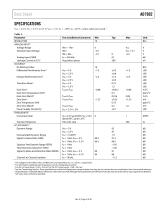
Data Sheet SPECIFICATIONS VDD = 2.5 V, VIO = 2.3 V to 5.5 V, VREF = 5 V, TA = −40°C to +125°C, unless otherwise noted. 1 Table 2. Parameter RESOLUTION ANALOG INPUT 2 Voltage Range Absolute Input Voltage Analog Input CMRR Leakage Current at 25°C ACCURACY No Missing Codes Differential Nonlinearity Error 3 Integral Nonlinearity Error3 Transition Noise3 Gain Error 4 Gain Error Temperature Drift Gain Error Match4 Zero Error4 Zero Temperature Drift Zero Error Match4 Power Supply Sensitivity3 THROUGHPUT Conversion Rate Transient Response AC ACCURACY 5 Dynamic Range Oversampled Dynamic Range Signal-to-Noise...
Open the catalog to page 4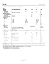
Data Sheet VDD = 2.5 V, VIO = 2.3 V to 5.5 V, TA = −40°C to +125°C, unless otherwise noted. 1 Table 3. Parameter REFERENCE Voltage Range Load Current SAMPLING DYNAMICS −3 dB Input Bandwidth Aperture Delay Aperture Delay Match DIGITAL INPUTS Logic Levels VIL VIH IIL IIH DIGITAL OUTPUTS Data Format Pipeline Delay VOL VOH POWER SUPPLIES VDDx VIOx VIOx Range IVDDx IVIOx Standby Current 2, 3 Power Dissipation VDDx Only REF Only VIO Only Energy per Conversion TEMPERATURE RANGE 4 Specified Performance Test Conditions/Comments 1 MSPS, VREF = 5 V, each ADC Bits Samples Straight binary No delay, conversion...
Open the catalog to page 5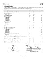
Data Sheet TIMING SPECIFICATIONS −40°C to +125°C, VDD = 2.37 V to 2.63 V, VIO = 2.3 V to 5.5 V, unless otherwise stated. See Figure 2 and Figure 3 for load conditions. See Figure 39, Figure 41, Figure 43, Figure 45, Figure 47, Figure 49, and Figure 51 for timing diagrams. Table 4. Parameter Conversion Time (CNVx Rising Edge to Data Available) Acquisition Time Time Between Conversions VIOx Above 2.3 V CNVx Pulse Width (CS Mode) SCKx Period (CS Mode) VIOx Above 4.5 V VIOx Above 3 V VIOx Above 2.7 V VIOx Above 2.3 V SCKx Period (Chain mode) VIOx Above 4.5 V VIOx Above 3 V VIOx Above 2.7 V VIOx Above...
Open the catalog to page 6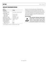
ABSOLUTE MAXIMUM RATINGS Analog Inputs Supply Voltage Digital Inputs toGND Digital Outputs toGND Storage Temperature Range Junction Temperature Lead Temperatures ' See the Analog Inputs section for an explanation of INx+ and INx- Data Sheet Stresses at or above those listed under Absolute Maximum Ratings may cause permanent damage to the product. This is a stress rating only; functional operation of the product at these or any other conditions above those indicated in the operational section of this specification is not implied. Operation beyond the maximum operating conditions for extended periods...
Open the catalog to page 7
Data Sheet PIN CONFIGURATION AND FUNCTION DESCRIPTIONS 20 Table 6. Pin Function Descriptions Pin No. 1, 6 Description Reference Input Voltage. The REFx range is 2.4 V to 5.1 V. These pins are referred to the GND pin, and decouple each pin closely to the GND pin with a 10 µF capacitor. Power Supplies. Pseudo Differential Positive Analog Inputs. Pseudo Differential Negative Analog Inputs. Power Supply Ground. Conversion Inputs. These inputs have multiple functions. On the leading edge, they initiate conversions and select the interface mode of the device: chain mode or active low chip select mode...
Open the catalog to page 8All Analog Devices catalogs and technical brochures
 HMC722LP3E
8 Pages
 Isolated Sigma-Delta Modulator
17 Pages
 HMC853 Data Sheet
10 Pages
 AN-1084
8 Pages
 AN-1091
2 Pages
 AN_737
8 Pages
 AN-0982
4 Pages
 ADF7024
24 Pages
 AD9915
48 Pages
 AD9914
48 Pages
 ADRF6612
59 Pages
 ADRF6820
48 Pages
 ADL5246
32 Pages
 ADA4961
22 Pages
 AN-1141
8 Pages
 AN-698
36 Pages
 Temperature Sensors
2 Pages
 Reference Circuits
8 Pages
 Precision ADCs
16 Pages
 ADR02ACHIPS: ADR02ACHIPS
8 Pages
 AD9364 RF Agile Transceiver
32 Pages
 Digital Temperature Sensors
2 Pages
 Digital to Analog Converter ICs
12 Pages
 AD1836A: Multichannel 96 kHz Codec
24 Pages


Archived catalogs
 Zero-Drift Amplifiers
2 Pages
 Powering ADI Components
8 Pages


- Ethernet switch
- Industrial network switch
- Acceleration sensor
- Unmanaged switch
- Transceiver module
- Analog Devices motor controller
- Triaxial acceleration sensor
- DC motor controller
- Data acquisition unit
- Analog Devices stepper motor controller
- Industrial converter
- Ethernet transceiver
- Processor
- High-voltage amplifier
- Low-noise amplifier
- Multiplexer
- Compact motor controller
- Gyroscope
- Closed-loop motor controller