- Catalogs
- Analog Devices
- AD7578: CMOS 12-Bit Siccessive Approximation ADC
AD7578: CMOS 12-Bit Siccessive Approximation ADC
1 /12Pages

AD7578: CMOS 12-Bit Siccessive Approximation ADC
1 /12Pages
Catalog excerpts
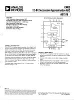
No Missed Codes Over Full Temperature Range Low Total Unadjusted Error ± 1LSB max High Impedance Analog Input Autozero Cycle for Low Offset Voltage Small Size: 0.3", 24-Pin Package GENERAL DESCRIPTION The AD7578 is a medium speed, monolithic 12-bit CMOS A/D converter which uses the successive approximation technique to provide a conversion time of lOOjxs. An auto-zero cycle occurs at the start of each conversion resulting in very low system offset voltages, typically less than lOOp-V. The device is designed for easy microprocessor interfacing using standard control signals; CS (decoded device address), RD (READ) and WR (WRITE). Conversion results are available in two bytes, 8LSBs and 4MSBs, over an 8-bit three state output bus. Either byte can be read first. Two converter busy flags are available to facilitate polling The analog input voltage range is OV to + 5V when using a FUNCTIONAL BLOCK DIAGRAM PRODUCT HIGHLIGHTS package requiring only a few passive components and a voltage 2. Autozero cycle realizes very low offset voltages, typically 3. Standard microprocessor control signals to allow easy inter- facing to most popular 8- and 16-bit microprocessors. 4. Monolithic construction for increased reliability and small Information furnished by Analog Devices is believed to be accurate and reliable. However, no responsibility is assumed by Analog Devices for its use, nor for any infringements of patents or other rights of third parties which may result from its use. No license is granted by implication or otherwise under any patent or patent rights of Analog Devices.
Open the catalog to page 1
all specifications TMIN to TMAX unless otherwise noted.) Differential Nonlinearity Full Scale Error (Gain Error)3 No missing codes guaranteed Full Scale TC is typically lppm/°C Offset Error TC is typically lppm/°C ANALOG INPUT Analog Input Range CAIN) Input Capacitance IAINJ Input Leakage Current REFERENCE INPUT VREF (For Specified Performance) VREF Range VREF Input Reference Current Degraded transfer accuracy POWER SUPPLY REJECTION LOGIC INPUTS _ VIH Input High Voltage VIH, Input High Voltage IIH, Input High Current LOGIC OUTPUTS V0H) Output High Voltage Floating State Leakage Current Floating...
Open the catalog to page 2
CStoWR Setup Time WR Pulse Width (Internal Clock Operation) WR Pulse Width (External Clock Operation) CStoWR Hold Time WRto BUSY Propagation Delay BUSY to CS Setup Time CStoRD Hold Time BYSLtoRD Setup Time BYSL to RD Hold Time RD to Valid Data (Bus Access Time) RD to Three State Output 'Timing Specifications are guaranteed by design, not production tested. All input control signals are specified with tr = tf=20ns (10% to 90% of + 5V) and timed from a voltage level of + 1.6V. Data is timed from 2When using an external clock source the WR pulse width must be extended to provide the minimum auto-zero...
Open the catalog to page 3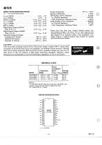
ABSOLUTE MAXIMUM RATINGS* (TA = + 25°C unless otherwise stated) Digital Input Voltage to DGND Digital Output Voltage to DGND Operating Temperature Range *Stresses above those listed under "Absolute Maximum Ratings" may cause permanent damage to the device. This is a stress rating only and functional operation of the device at these or any other conditions above those indicated in the operational sections of this specification is not implied. Exposure to absolute maximum rating conditions for extended periods may affect device reliability. ESD (electrostatic discharge) sensitive device. Electrostatic...
Open the catalog to page 4
Autozero Capacitor Input. Connect other side of capacitor to AGND. Analog Input Voltage reference input. The AD7578 is specified with VREF = + 5.0V. Analog Ground Digital Ground Logic Supply. For VCc = + 5V digital inputs and outputs are TTL compatible. Three state data outputs. They become active when CS & RD are brought low. Individual pin function is dependent upon the Byte Select (BYSL) input. 'BUSY (Pin 8) is a converter status flag and is HIGH during a conversion. 2Pins 9-11 output a logic LOW when BYSL is HIGH. DBll-DBOarethe 12-bit conversion results, DB11 is the MSB. READ input. This...
Open the catalog to page 5
Operating Information OPERATIONAL DIAGRAM An operational diagram for the AD7578 is shown in Figure 5. The only passive components required are the autozero capacitor CAZ and timing components RCLK, CCLKI & CCLK2 for the internal clock oscillator. If the AD7578 is to be used with an external clock source, then only CAZ is required. Individual pin functions are described in detail on the previous page. ANALOG INPUT Figure 5. AD7578 Operational Diagram INTERNAL CLOCK OPERATION The clock circuitry for internal clock operation is shown in Figure 6 and the AD7578 operating waveforms are shown in Figure...
Open the catalog to page 6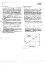
READING DATA The 12-bit conversion data plus a converter status flag are available over an 8-bit wide data bus. Data is transferred from the AD7578 in right-justified format (i.e., the LSB is the most right-hand bit in a 16-bit word). Two READ operations are required, the Byte Select (BYSL) input determining which byte-8 least significant bits or 4 most significant bits plus status flag-is to be read first. Since the AD7578 uses the successive approximation register (SAR) to hold conversion results (refer to Functional Diagram), it is necessary to wait until a conversion is finished before reading...
Open the catalog to page 7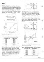
The high input impedance of the analog input, AIN, allows simple analog interfacing. Zero to + 5V signal sources can be connected directly to the analog input without additional buffering for source impedances up to 5kfi (see Figure 11). The input/output transfer characteristic and transition points for this input signal range are shown in Figure 12 and Table I respectively. The designed transition points on the AD7578 transfer characteristic occur on integer multiples of 1LSB. The output code is Natural * ADDITIONAL PINS OMITTED FOR CLARITY Figure 11. Unipolar 0 to +5V Operation ANALOG INPUT....
Open the catalog to page 8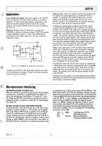
Power Supply Decoupling: All power supplies to the AD7578 should be bypassed with either lOuP tantulum or electrolytic capacitors. To ensure good high frequency performance, each capacitor should be bypassed with an 0.0lap disc ceramic capacitor. All capacitors should be placed as close as possible to Reference Circuit: Figure 16 shows how to configure an AD584LH to produce a reference voltage of 5.00V. R2 provides a typical adjustment range of ± 75mV. The AD584LH will contribute less than 1LSB of gain error over the commercial temperature range. Figure 16. AD584LH as Reference Generator Transient...
Open the catalog to page 9All Analog Devices catalogs and technical brochures
 HMC722LP3E
8 Pages
 Isolated Sigma-Delta Modulator
17 Pages
 HMC853 Data Sheet
10 Pages
 AN-1084
8 Pages
 AN-1091
2 Pages
 AN_737
8 Pages
 AN-0982
4 Pages
 ADF7024
24 Pages
 AD9915
48 Pages
 AD9914
48 Pages
 ADRF6612
59 Pages
 ADRF6820
48 Pages
 ADL5246
32 Pages
 ADA4961
22 Pages
 AN-1141
8 Pages
 AN-698
36 Pages
 Temperature Sensors
2 Pages
 Reference Circuits
8 Pages
 Precision ADCs
16 Pages
 ADR02ACHIPS: ADR02ACHIPS
8 Pages
 AD9364 RF Agile Transceiver
32 Pages
 Digital Temperature Sensors
2 Pages
 Digital to Analog Converter ICs
12 Pages
 AD1836A: Multichannel 96 kHz Codec
24 Pages


Archived catalogs
 Zero-Drift Amplifiers
2 Pages
 Powering ADI Components
8 Pages


- Ethernet switch
- Industrial network switch
- Acceleration sensor
- Unmanaged switch
- Transceiver module
- Analog Devices motor controller
- Triaxial acceleration sensor
- DC motor controller
- Data acquisition unit
- Analog Devices stepper motor controller
- Industrial converter
- Ethernet transceiver
- Processor
- High-voltage amplifier
- Low-noise amplifier
- Multiplexer
- Compact motor controller
- Gyroscope
- Closed-loop motor controller
- Digital converter