- Catalogs
- Analog Devices
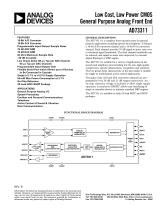
- AD73311: Low Cost, Low Power CMOS General Purpose Analog Front End Data Sheet
AD73311: Low Cost, Low Power CMOS General Purpose Analog Front End Data Sheet
1 /36Pages

AD73311: Low Cost, Low Power CMOS General Purpose Analog Front End Data Sheet
1 /36Pages
Catalog excerpts
Low Cost, Low Power CMOS General Purpose Analog Front End AD73311 FEATURES 16-Bit A/D Converter 16-Bit D/A Converter Programmable Input/Output Sample Rates 75 dB ADC SNR 70 dB DAC SNR 64 kS/s Maximum Sample Rate –90 dB Crosstalk Low Group Delay (25 s Typ per ADC Channel, 50 s Typ per DAC Channel) Programmable Input/Output Gain Flexible Serial Port which Allows up to 8 Devices to Be Connected in Cascade Single (+2.7 V to +5.5 V) Supply Operation 50 mW Max Power Consumption at 2.7 V On-Chip Reference 20-Lead SOIC/SSOP Package GENERAL DESCRIPTION The AD73311 is a complete front-end processor for general purpose applications including speech and telephony. It features a 16-bit A/D conversion channel and a 16-bit D/A conversion channel. Each channel provides 70 dB signal-to-noise ratio over a voiceband signal bandwidth. The final channel bandwidth can be reduced, and signal-to-noise ratio improved, by external digital filtering in a DSP engine. The AD73311 is suitable for a variety of applications in the speech and telephony area including low bit rate, high quality compression, speech enhancement, recognition and synthesis. The low group delay characteristic of the part makes it suitable for single or multichannel active control applications. The gains of the A/D and D/A conversion channels are programmable over 38 dB and 21 dB ranges respectively. An on-chip reference voltage is included to allow single supply operation. A serial port (SPORT) allows easy interfacing of single or cascaded devices to industry standard DSP engines. APPLICATIONS General Purpose Analog I/O Speech Processing Cordless and Personal Communications Telephony Active Control of Sound & Vibration Data Communications The AD73311 is available in both 20-lead SOIC and SSOP packages. FUNCTIONAL BLOCK DIAGRAM AVDD1 ANALOG SIGMA-DELTA MODULATOR DECIMATOR SCLK VINN SERIAL I/O PORT VOUTP +6/–15dB PGA VOUTN REFCAP CONTINUOUS TIME LOW-PASS FILTER SWITCHEDCAPACITOR LOW-PASS FILTER DIGITAL SIGMA-DELTA MODULATOR SDO SDOFS SE MCLK RESET REV. B Information furnished by Analog Devices is believed to be accurate and reliable. However, no responsibility is assumed by Analog Devices for its use, nor for any infringements of patents or other rights of third parties which may result from its use. No license is granted by implication or otherwise under any patent or patent rights of Analog Devices. One Technology Way, P.O. Box 9106, Norwood, MA 02062-9106, U.S.A. Tel: 781/329-4700 World Wide Web Site: http://www.analog.com Fax: 781/326-8703 © Analog Devices, Inc., 2000
Open the catalog to page 1
+3 DVDD +3 V 10%; DGND = AGND AD73311–SPECIFICATIONS1 (AVDD64=kHz;VT؎=10%; to T =, unless؎otherwise noted) = 0 V, f F = T Parameter REFERENCE REFCAP Absolute Voltage, VREFCAP REFCAP TC REFOUT Typical Output Impedance Absolute Voltage, VREFOUT Minimum Load Resistance Maximum Load Capacitance Total Harmonic Distortion PGA = 0 dB PGA = 38 dB Intermodulation Distortion Idle Channel Noise Crosstalk DC Offset Power Supply Rejection Differential Nominal Voltage Output Swing (0 dBm0) Single-Ended Differential Total Harmonic Distortion PGA = 0 dB PGA = 6 dB Intermodulation Distortion Idle Channel Noise...
Open the catalog to page 2
AD73311 Parameter DAC SPECIFICATIONS (Continued) Power Supply Rejection LOGIC INPUTS VINH, Input High Voltage VINL, Input Low Voltage IIH, Input Current CIN, Input Capacitance Test Conditions/Comments Output DC Offset 2, 7 Minimum Load Resistance, R L2, 8 Single-Ended Differential Maximum Load Capacitance, CL2, 8 Single-Ended Differential FREQUENCY RESPONSE (ADC AND DAC)9 Typical Output 0 Hz 2000 Hz 4000 Hz 8000 Hz 12000 Hz 16000 Hz 20000 Hz 24000 Hz 28000 Hz > 32000 Hz Input Signal Level at AVDD and DVDD Pins: 1.0 kHz, 100 mV p-p Sine Wave 64 kHz Input Sample Rate, Interpolator Bypassed (CRE:5...
Open the catalog to page 3
+5 +5 V 10%; DGND = AGND AD73311–SPECIFICATIONS1 (AVDD64=kHz;VT؎=10%; DVDD =, unless؎otherwise noted) = 0 V, f F = T to T Minimum Load Resistance Maximum Load Capacitance ADC SPECIFICATIONS Maximum Input Range at VIN2, 3 Test Conditions/Comments 5VEN = 0 5VEN = 1 0.1 µF Capacitor Required from REFCAP to AGND2 REFCAP TC REFOUT Typical Output Impedance Absolute Voltage, V REFOUT REFERENCE REFCAP Absolute Voltage, V REFCAP 1.0 kHz, 0 dBm0 1.0 kHz, 0 dBm0 1.0 kHz, +3 dBm0 to –50 dBm0 Refer to Figure 5 300 Hz to 3.4 kHz Frequency Range 0 Hz to 32 kHz Frequency Range 300 Hz to 3.4 kHz Frequency Range...
Open the catalog to page 4
Test Conditions/Comments Output DC Offset 2, 7 Minimum Load Resistance, R L2, 8 Single-Ended Differential Maximum Load Capacitance, CL2, 8 Single-Ended Differential Input Signal Level at AVDD and DVDD Pins: 1.0 kHz, 100 mV p-p Sine Wave 64 kHz Input Sample Rate, Interpolator Bypassed (CRE:5 = 1) PGA = 6 dB DAC SPECIFICATIONS (Continued) Power Supply Rejection FREQUENCY RESPONSE (ADC AND DAC)9 Typical Output 0 Hz 2000 Hz 4000 Hz 8000 Hz 12000 Hz 16000 Hz 20000 Hz 24000 Hz 28000 Hz > 32000 Hz LOGIC INPUTS VINH, Input High Voltage VINL, Input Low Voltage IIH, Input Current CIN, Input Capacitance...
Open the catalog to page 5
AD73311 Table II. Current Summary (AVDD = DVDD = +5.5 V) Internal Digital Current 6 6 0 External Interface Current 2 2 0 Conditions ADC On Only ADC and DAC On REFCAP On Only REFCAP and REFOUT On Only All Sections Off Comments REFOUT Disabled REFOUT Disabled REFOUT Disabled MCLK Active Levels Equal to 0 V and DVDD Digital Inputs Static and Equal to 0 V or DVDD The above values are in mA and are typical values unless otherwise noted. Table III. Signal Ranges Maximum Input Range at VIN Nominal Reference Level Maximum Voltage Output Swing Single-Ended Differential Nominal Voltage Output Swing Single-Ended...
Open the catalog to page 6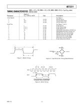
AD73311 (AVDD = +5 V ؎ 10%; DVDD = +5 V ؎ 10%; AGND = DGND = 0 V; TA = TMlN to TMAX, unless otherwise noted) TIMING CHARACTERISTICS Parameter See Figure 1 MCLK Period MCLK Width High MCLK Width Low See Figures 3 and 4 SCLK Period SCLK Width High SCLK Width Low SDI/SDIFS Setup Before SCLK Low SDI/SDIFS Hold After SCLK Low SDOFS Delay from SCLK High SDOFS Hold After SCLK High SDO Hold After SCLK High SDO Delay from SCLK High SCLK Delay from MCLK * SCLK IS INDIVIDUALLY PROGRAMMABLE IN FREQUENCY (MCLK/4 SHOWN HERE). Figure 3. SCLK Timing Figure 2. Load Circuit for Timing Specifications Figure 1....
Open the catalog to page 7All Analog Devices catalogs and technical brochures
 HMC722LP3E
8 Pages
 Isolated Sigma-Delta Modulator
17 Pages
 HMC853 Data Sheet
10 Pages
 AN-1084
8 Pages
 AN-1091
2 Pages
 AN_737
8 Pages
 AN-0982
4 Pages
 ADF7024
24 Pages
 AD9915
48 Pages
 AD9914
48 Pages
 ADRF6612
59 Pages
 ADRF6820
48 Pages
 ADL5246
32 Pages
 ADA4961
22 Pages
 AN-1141
8 Pages
 AN-698
36 Pages
 Temperature Sensors
2 Pages
 Reference Circuits
8 Pages
 Precision ADCs
16 Pages
 ADR02ACHIPS: ADR02ACHIPS
8 Pages
 AD9364 RF Agile Transceiver
32 Pages
 Digital Temperature Sensors
2 Pages
 Digital to Analog Converter ICs
12 Pages
 AD1836A: Multichannel 96 kHz Codec
24 Pages


Archived catalogs
 Zero-Drift Amplifiers
2 Pages
 Powering ADI Components
8 Pages


- Ethernet switch
- Industrial network switch
- Acceleration sensor
- Unmanaged switch
- Transceiver module
- Analog Devices motor controller
- Triaxial acceleration sensor
- DC motor controller
- Data acquisition unit
- Analog Devices stepper motor controller
- Industrial converter
- Ethernet transceiver
- High-voltage amplifier
- Low-noise amplifier
- Multiplexer
- Compact motor controller
- Gyroscope
- Closed-loop motor controller
- Digital converter