
- Catalogs
- Analog Devices
- AD7262: 1 MSPS, 12-Bit, Simultaneous Sampling SAR ADC with PGA and Four Comparators Data Sheet


- Products
- Catalogs
- News & Trends
- Exhibitions
AD7262: 1 MSPS, 12-Bit, Simultaneous Sampling SAR ADC with PGA and Four Comparators Data Sheet
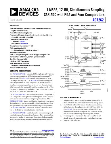
AD7262: 1 MSPS, 12-Bit, Simultaneous Sampling SAR ADC with PGA and Four Comparators Data Sheet
The AD7262 is a dual, 12-bit, high-speed, low-power successive approximation ADC designed for simultaneous sampling and conversion of two channels. It operates from a single 5 V power supply and is suitable for monitoring small amplitude signals from various sensors, particularly in motor control systems.
The AD7262 features a throughput rate of up to 1 MSPS per ADC, while the AD7262-5 offers up to 500 kSPS. It includes a programmable gain stage with 14 settings ranging from ×1 to ×128, allowing for flexible detection and conversion of low-level analog signals. The device operates over a temperature range of -40°C to +105°C and includes an on-chip 2.5 V reference, which can be disabled for external reference use.
The ADCs are preceded by true differential analog inputs with a programmable gain amplifier (PGA). The device also includes four comparators, with two optimized for low power and two for fast propagation delays. Calibration functions are available to remove device offset errors and adjust gain for input path compensation.
The AD7262 offers a signal-to-noise ratio (SNR) of 73 dB at a gain of 2 and 66 dB at a gain of 32. It provides a wide input bandwidth with a -3 dB bandwidth of 1.7 MHz at a gain of 2. The device ensures no missed codes to 12 bits and features a high-speed serial interface compatible with SPI/QSPI/MICROWIRE/DSP.
The AD7262 is ideal for applications requiring simultaneous sampling, such as motor control systems, where it can monitor position feedback signals from analog encoders. It is also suitable for other sensor monitoring applications due to its high input impedance and flexible gain settings.
The AD7262 provides a comprehensive solution for high-speed, low-power analog-to-digital conversion with integrated features that enhance its applicability in various sensor monitoring and control systems.
The document outlines the absolute maximum ratings for the AD7262, including voltage limits for various pins, operating and storage temperature ranges, and thermal impedance values for different package types. Exceeding these ratings may cause permanent damage to the product.
The AD7262 features a 48-lead LQFP and LFCSP package with detailed pin descriptions. Key pins include AVCC for analog supply voltage, CA_CBVCC and CC_CDVCC for comparator supply voltage, and various analog and digital input/output pins. Proper decoupling and grounding are emphasized for optimal performance.
The document provides graphs illustrating the typical performance of the AD7262, including Differential Nonlinearity (DNL), Integral Nonlinearity (INL), Signal-to-Noise Ratio (SNR), and Total Harmonic Distortion (THD) across different gain settings. These characteristics are measured under specific conditions such as AVCC and VDRIVE voltages, sampling frequency, and temperature.
Definitions for key terms such as Differential Nonlinearity (DNL), Integral Nonlinearity (INL), Zero Code Error, and Full-Scale Error are provided to aid in understanding the performance metrics of the AD7262.
The AD7262/AD7262-5 feature two on-chip differential programmable gain amplifiers, two track-and-hold amplifiers, and two successive approximation ADCs with a serial interface. They also include four on-chip comparators and require specific power supplies for operation. The PGA allows selection from 14 programmable gain stages, accepting fully differential analog signals.
Each ADC has two high impedance differential analog inputs. The input structure includes ESD protection diodes and capacitors. The document provides a table detailing the analog input range for various PGA gain settings.
The AD7262/AD7262-5 can operate with either an internal 2.5 V on-chip reference or an externally applied reference. The REFSEL pin determines the reference source.
The ADCs use control logic, a SAR, and capacitive DACs for conversion. The PGA features high analog input impedance and true differential analog inputs, allowing direct connection from sources or sensors.
The AD7262/AD7262-5 include four on-chip comparators, with two featuring ultralow power consumption and two with fast propagation delays. They are suitable for monitoring signals in motor control systems.
The document provides diagrams for typical connections, illustrating configurations for control register mode and pin-driven mode, including power supply and reference connections.
The comparators are designed without internal hysteresis, allowing users to add external hysteresis if needed. The document provides equations and examples for selecting external resistor and capacitor values to achieve the desired hysteresis level, which is crucial for stability in noisy environments.
The devices are tailored for motor control shaft position feedback loops and can interface directly with various sensors. The ADCs sample sine and cosine outputs from sensors, and the on-chip comparators monitor pole sensors.
The AD7262/AD7262-5 can operate in pin-driven mode or control register mode. Pin-driven mode allows users to select gain, power-down modes, and initiate calibration via logic levels on specific pins. Control register mode provides similar functionalities through a 12-bit read/write register.
Multiple power-down options are available to optimize power dissipation. These modes can be selected via control register programming or by setting specific pin logic levels. The document outlines configurations for powering down comparators and ADCs independently.
On power-up, the status of gain pins determines the operational mode. In pin-driven mode, appropriate logic states must be configured, and calibration initiated if necessary. In control register mode, comparators and ADCs are powered down by default.
The control register is a 12-bit register used to control device functions when not in pin-driven mode. It allows selection of PGA gain, power-down modes, and calibration. Data is loaded via the PD0/DIN pin, and specific timing diagrams are provided for write operations.
The AD7262/AD7262-5 contain a control register, offset registers for each ADC, and external gain registers. These registers are read/write accessible, and the document provides detailed instructions for addressing and writing to these registers.
The document provides detailed instructions on configuring and operating the AD7262/AD7262-5 ADCs. It includes procedures for writing to and reading from control registers, which involve specific bit sequences to reset and configure the ADC for future conversions. The document also describes the serial interface, detailing the timing diagrams for data transfer using SCLK and CS signals. The ADCs require a minimum of 19 SCLKs for conversion, and data can be read on either the rising or falling edge of the SCLK, depending on the frequency used.
The AD7262/AD7262-5 supports internal offset calibration, which can be initiated using the CAL pin or through the control register. Calibration requires one full conversion cycle and is necessary when changing the PGA gain to ensure accuracy. The document provides a method for manually adjusting the offset calibration registers to compensate for signal path offsets.
The ADCs allow for system gain calibration by writing to external gain registers, enabling the removal of system gain errors. Each ADC has independent gain registers, and the gain calibration feature can be used to match gains between ADCs. The gain register contains seven bits, with a sign bit and six bits for the multiplication factor.
The AD7262/AD7262-5 can interface directly with various microprocessors, including the Blackfin DSP family. The document provides configuration settings for interfacing with the ADSP-BF531, detailing the necessary register settings for the SPORT0 Receive Configuration.
The document emphasizes the importance of proper grounding and layout to minimize coupling between analog and digital sections. It suggests separate pinning for analog and digital supplies to reduce interference.
For optimal performance of the AD7262/AD7262-5, it is crucial to separate the analog and digital sections on the PCB. This separation allows for distinct ground planes, which should be connected at a single star ground point near the device's ground pins. Avoid running digital lines under the device to prevent noise coupling, while allowing the analog ground plane to run beneath it. Power supply lines should be as wide as possible to minimize impedance and glitches.
Fast switching signals, such as clocks, should be shielded with digital ground and kept away from analog inputs. Digital and analog signals should not cross over each other. For double-sided boards, a microstrip technique is recommended, dedicating one side to ground planes and the other to signals.
All analog supplies should be decoupled with 10 μF tantalum capacitors in parallel with 100 nF capacitors placed close to the device. These capacitors should have low ESR and ESI to provide a low impedance path to ground at high frequencies.
The PCB pad for the chip scale package should be slightly larger than the package land to maximize solder joint size. The thermal pad on the PCB should match the size of the exposed pad on the package, with a clearance of at least 0.25 mm to prevent shorting. Thermal vias should be used to enhance thermal performance, with specific dimensions and copper plating requirements.
The document provides detailed dimensions for the 48-Lead Lead Frame Chip Scale Package (LFCSP_VQ) and the 48-Lead Low Profile Quad Flat Package (LQFP), compliant with JEDEC standards.
The document lists various models of the AD7262, specifying temperature ranges, package descriptions, and options, including evaluation and development boards.
Catalog excerpts
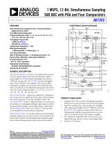
FUNCTIONAL BLOCK DIAGRAM Dual simultaneous sampling 12-bit, 2-channel analog-todigital converter (ADC) True differential analog inputs Programmable gain stage: ×1, ×2, ×3, ×4, ×6, ×8, ×12, ×16, ×24, ×32, ×48, ×64, ×96, ×128 Throughput rate per ADC 1 MSPS for AD7262 500 kSPS for AD7262-5 Analog input impedance: >1 GΩ Wide input bandwidth −3 dB bandwidth: 1.7 MHz at gain = 2 4 on-chip comparators SNR: 73 dB typical at gain = 2, 66 dB typical at gain = 32 Device offset calibration, system gain calibration On-chip reference: 2.5 V −40°C to +105°C operation High speed serial interface SPI/QSPI™/MICROWIRE/DSP compatible 48-lead LFCSP and LQFP OUTPUT DRIVERS The AD7262/AD7262-5 are ideally suited for monitoring small amplitude signals from a variety of sensors. They include all the functionality needed for monitoring the position feedback signals from a variety of analog encoders used in motor control systems. OUTPUT DRIVERS SCLK CAL CS REFSEL G0 G1 G2 G3 VDRIVE The AD7262/AD7262-5 contain four comparators. Comparator A and Comparator B are optimized for low power, while Comparator C and Comparator D have fast propagation delays. The AD7262/AD7262-5 feature a calibration function to remove any device offset error and programmable gain adjust registers to allow for input path (for example, sensor) offset and gain compensation. The AD7262/AD7262-5 have an on-chip 2.5 V reference that can be disabled if an external reference is preferred. CONTROL LOGIC GENERAL DESCRIPTION The AD7262/AD7262-5 are dual, 12-bit, high speed, low power, successive approximation ADCs that operate from a single 5 V power supply. The AD7262 features throughput rates of up to 1 MSPS per on-chip ADC. The AD7262-5 features throughput rates of up to 500 kSPS. Two complete ADC functions allow simultaneous sampling and conversion of two channels. Each ADC is preceded by a true differential analog input with a PGA. There are 14 gain settings available: ×1, ×2, ×3, ×4, ×6, ×8, ×12, ×16, ×24, ×32, ×48, ×64, ×96, and ×128. OUTPUT DRIVERS COUTA OUTPUT DRIVERS OUTPUT DRIVERS COUTC OUTPUT DRIVERS Integrated PGA with a variety of flexible gain settings to allow detection and conversion of low level analog signals. Each PGA is followed by a dual simultaneous sampling ADC, featuring throughput rates of 1 MSPS per ADC for the AD7262. The conversion results of both ADCs are simultaneously available on separate data lines or in succession on one data line if only one serial port is available. Four integrated comparators that can be used to count signals from pole sensors in motor control applications. Internal 2.5 V reference. Document Feedback Information furnished by Analog Devices is believed to be accurate and reliable. However, no responsibility is assumed by Analog Devices for its use, nor for any infringements of patents or other rights of third parties that may result from its use. Specifications subject to change without notice. No license is granted by implication or otherwise under any patent or patent rights of Analog Devices. Trademarks and registered trademarks are the property of their respective owners. One Technology Way, P.O. Box 9106, Norwood, MA 02062-9106, U.S.A. Tel: 781.329.4700 ©2008–2015 Analog Devices, Inc. All rights reserved. Technical Support www.analog.com Data Sheet 1 MSPS, 12-Bit, Simultaneous Sampling SAR ADC with PGA and Four Comparators AD7262
Open the catalog to page 1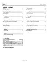
Data Sheet
Open the catalog to page 2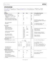
Data Sheet SPECIFICATIONS AVCC = 4.75 V to 5.25 V, CA_CBVCC = CC_CDVCC = 2.7 V to 5.25 V, VDRIVE = 2.7 V to 5.25 V, fSAMPLE = 1 MSPS and fSCLK = 40 MHz for AD7262, fSAMPLE = 500 kSPS and fSCLK = 20 MHz for AD7262-5, VREF = 2.5 V internal/external; TA = −40°C to +105°C, unless otherwise noted. Table 1. Parameter DYNAMIC PERFORMANCE1 Signal-to-Noise Ratio (SNR)2 Signal-to-(Noise + Distortion) Ratio (SINAD)2 Total Harmonic Distortion (THD)2 Spurious-Free Dynamic Range (SFDR)2 Common-Mode Rejection Ratio (CMRR)3 Positive Full-Scale Error Match Zero Code Error2 Zero Code Error Match Negative Full-Scale...
Open the catalog to page 3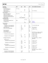
AD7262 Parameter LOGIC INPUTS Input High Voltage, VINH Input Low Voltage, VINL Input Current, IIN Input Capacitance, CIN3 LOGIC OUTPUTS Output High Voltage, VOH Output Low Voltage, VOL Floating State Leakage Current Floating State Output Capacitance3 Output Coding CONVERSION RATE Conversion Time Track-and-Hold Acquisition Time Throughput Rate COMPARATORS Input Offset Comparator A and Comparator B Comparator C and Comparator D Offset Voltage Drift Input Common-Mode Range3 Input Capacitance3 Input Impedance3 IDD Normal Mode (Static) 6 Comparator A and Comparator B Comparator C and Comparator D...
Open the catalog to page 4
Data Sheet Parameter POWER REQUIREMENTS AVCC CA_CBVCC, CC_CDVCC VDRIVE IDD ADC Normal Mode (Static) ADC Normal Mode (Dynamic) Shutdown Mode Power Dissipation ADC Normal Mode (Static) ADC Normal Mode (Dynamic) Shutdown Mode Test Conditions/Comments Digital inputs = 0 V or VDRIVE AVCC = 5.25 V AVCC = 5.25 V AVCC = 5.25 V, ADCs and comparators powered down These specifications were determined without the use of the gain calibration feature. See the Terminology section. Samples tested during initial release to ensure compliance; they are not subject to production testing. 4 For PGA gain = 1; to use...
Open the catalog to page 5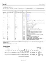
Data Sheet TIMING SPECIFICATIONS AVCC = 4.75 V to 5.25 V, CA_CBVCC = CC_CDVCC = 2.7 V to 5.25 V, VREF = 2.5 V internal/external; TA = TMIN to TMAX, unless otherwise noted. 1 Table 2. Parameter fSCLK Description AD7262 2 AD72622 AD7262-5 tSCLK = 1/fSCLK AD7262 AD7262-5 Minimum time between end of serial read/bus relinquish and next falling edge of CS CS to SCLK setup time Delay from 19th SCLK falling edge until DOUTA and DOUTB are three-state disabled Data access time after SCLK falling edge SCLK to data valid hold time SCLK high pulse width SCLK low pulse width CS rising edge to falling edge...
Open the catalog to page 6All Analog Devices catalogs and technical brochures
 HMC722LP3E
8 Pages
 Isolated Sigma-Delta Modulator
17 Pages
 HMC853 Data Sheet
10 Pages
 AN-1084
8 Pages
 AN-1091
2 Pages
 AN_737
8 Pages
 AN-0982
4 Pages
 ADF7024
24 Pages
 AD9915
48 Pages
 AD9914
48 Pages
 ADRF6612
59 Pages
 ADRF6820
48 Pages
 ADL5246
32 Pages
 ADA4961
22 Pages
 AN-1141
8 Pages
 AN-698
36 Pages
 Temperature Sensors
2 Pages
 Reference Circuits
8 Pages
 Precision ADCs
16 Pages
 ADR02ACHIPS: ADR02ACHIPS
8 Pages
 AD9364 RF Agile Transceiver
32 Pages
 Digital Temperature Sensors
2 Pages
 Digital to Analog Converter ICs
12 Pages
 AD1836A: Multichannel 96 kHz Codec
24 Pages




























Archived catalogs
 Zero-Drift Amplifiers
2 Pages
 Powering ADI Components
8 Pages




- Ethernet switch
- Industrial network switch
- Acceleration sensor
- Unmanaged switch
- Analog Devices motor controller
- Transceiver module
- Triaxial acceleration sensor
- DC motor controller
- Data acquisition unit
- Analog Devices stepper motor controller
- Industrial converter
- Ethernet transceiver
- Processor
- High-voltage amplifier
- Low-noise amplifier
- Multiplexer
- Compact motor controller
- Digital converter
- Closed-loop motor controller
- Digital motor controller