
- Catalogs
- Analog Devices
- AD5693R/AD5692R/AD5691R/AD5693: Tiny 16-/14-/12-Bit I2C nanoDAC+, with ±2 LSB INL (16-Bit) and 2 ppm/°C Reference


- Products
- Catalogs
- News & Trends
- Exhibitions
AD5693R/AD5692R/AD5691R/AD5693: Tiny 16-/14-/12-Bit I2C nanoDAC+, with ±2 LSB INL (16-Bit) and 2 ppm/°C Reference

AD5693R/AD5692R/AD5691R/AD5693: Tiny 16-/14-/12-Bit I2C nanoDAC+, with ±2 LSB INL (16-Bit) and 2 ppm/°C Reference
The AD5693R/AD5692R/AD5691R/AD5693 are ultra-small, low-power, single-channel DACs with high relative accuracy and low drift. They offer a selectable output span and robust ESD protection, suitable for diverse applications.
These DACs are ideal for process controls, data acquisition systems, digital gain and offset adjustment, programmable voltage sources, and optical modules.
Part of the nanoDAC+ family, these devices offer 16-/14-/12-bit resolution with a buffered voltage output, operating from a single 2.7 V to 5.5 V supply. The AD5693R/AD5692R/AD5691R models include an internal 2.5 V reference, while the AD5693 requires an external reference.
The DACs provide high static performance with low differential nonlinearity and total unadjusted error, supporting a wide operating temperature range and low power requirements.
They exhibit fast output voltage settling time, low digital-to-analog glitch impulse, and excellent total harmonic distortion performance.
Supporting a maximum serial clock frequency of 400 kHz, the DACs ensure reliable data communication with precise timing requirements.
Key highlights include high relative accuracy, low drift on-chip reference, and compact packaging options.
Includes timing diagrams for the I2C serial interface and reset/LDAC timing.
Specifies limits beyond which the device may suffer permanent damage, including VDD to GND: -0.3 V to +7 V, Operating Temperature Range: -40°C to +105°C, and ESD Protection: 4 kV (HBM).
Thermal resistance values indicate heat dissipation capabilities for different package types.
Details pin configurations for 10-Lead MSOP and 8-Lead LFCSP packages, describing each pin's function.
Graphs illustrate performance metrics like Integral Nonlinearity (INL), Differential Nonlinearity (DNL), and Total Unadjusted Error (TUE).
Definitions for key terms such as INL, DNL, Zero Code Error, and Full-Scale Error.
Offset error is measured with specific codes in the DAC register for different models.
Measures the effect of supply voltage changes on the DAC output.
Time required for the DAC output to stabilize after an input change.
Measured as the area of the glitch during a major carry transition.
Measures the impulse injected into the analog output from the digital inputs.
Characterizes internally generated random noise.
Frequency at which the output amplitude falls to 3 dB below the input.
Measures the difference between an ideal sine wave and its attenuated version using the DAC.
Measures the change in reference output voltage with temperature changes.
Describes the operation of the DACs, including data writing via an I2C serial interface and power-on reset circuit.
Uses straight binary input coding with specific equations for each model.
Implements a segmented string architecture with an internal output buffer.
The on-chip reference can be disabled for external reference use.
A rail-to-rail design with a gain settable to ×1 or ×2.
Features a 2-wire, I2C-compatible serial interface.
Describes the process for write and read operations.
Offers normal and power-down modes with selectable output impedance.
Allows setting power-down and gain functions, enabling/disabling the internal reference, and performing a software reset.
Describes the update process for the DAC register, input register, and output.
The RESET signal resets the DAC output to zero-scale and sets registers to default values.
Voltage difference on the reference voltage due to temperature changes.
Describes the recommended power-up sequence to avoid unintentional powering.
Emphasizes careful power supply and ground return layout for accuracy.
Provides dimensions for the 8-Lead LFCSP and 10-Lead MSOP packages.
Lists various models with specifications such as resolution, temperature range, and package description.
Catalog excerpts

Tiny 16-/14-/12-Bit I2C nanoDAC+, with ±2 LSB INL (16-Bit) and 2 ppm/°C Reference Data Sheet FUNCTIONAL BLOCK DIAGRAM Ultrasmall package: 2 mm × 2 mm, 8-lead LFCSP High relative accuracy (INL): ±2 LSB maximum at 16 bits AD5693R/AD5692R/AD5691R Low drift, 2.5 V reference: 2 ppm/°C typical Selectable span output: 2.5 V or 5 V AD5693 External reference only Selectable span output: VREF or 2 × VREF Total unadjusted error (TUE): ±0.06% of FSR maximum Offset error: ±1.5 mV maximum Gain error: ±0.05 % of FSR maximum Low glitch: 0.1 nV-sec High drive capability: 20 mA Low power: 1.2 mW at 3.3 V Independent logic supply: 1.8 V to 5.5 V Wide operating temperature range: −40°C to +105°C Robust 4 kV HBM ESD protection POWER-ON RESET INPUT CONTROL LOGIC OUTPUT BUFFER POWER-DOWN CONTROL LOGIC RESISTOR NETWORK Figure 1. MSOP VREF POWER-ON RESET Process controls Data acquisition systems Digital gain and offset adjustment Programmable voltage sources Optical modules INPUT CONTROL LOGIC OUTPUT BUFFER POWER-DOWN CONTROL LOGIC RESISTOR NETWORK GENERAL DESCRIPTION The internal power-on reset circuit ensures that the DAC register is written to zero scale at power-up while the internal output buffer is configured in normal mode. The AD5693R/AD5692R/ AD5691R/AD5693 contain a power-down mode that reduces the current consumption of the device to 2 µA (maximum) at 5 V and provides software selectable output loads. The AD5693R/AD5692R/AD5691R/AD5693 use an I2C interface. Some device options also include an asynchronous RESET pin and a VLOGIC pin, allowing 1.8 V compatibility. Rev. A The AD5693R/AD5692R/AD5691R/AD5693, members of the nanoDAC+® family, are low power, single-channel, 16-/14-/ 12-bit buffered voltage output DACs. The devices, except the AD5693, include an enabled by default internal 2.5 V reference, offering 2 ppm/°C drift. The output span can be programmed to be 0 V to VREF or 0 V to 2 × VREF. All devices operate from a single 2.7 V to 5.5 V supply and are guaranteed monotonic by design. The devices are available in a 2.00 mm × 2.00 mm, 8-lead LFCSP or a 10-lead MSOP. NOTES 1. NOT ALL PINS AVAILABLE IN ALL 8-LEAD LFCSP MODELS. 2. NOT AVAILABLE IN THE AD5693. Table 1. Related Devices Interface SPI I2 C Reference Internal External Internal External High relative accuracy (INL): ±2 LSB maximum (AD5693R/AD5693, 16-bit). Low drift, 2.5 V on-chip reference: 2 ppm/°C typical and 5 ppm/°C maximum temperature coefficient. 2 mm × 2 mm, 8-lead LFCSP and 10-lead MSOP. Document Feedback Information furnished by Analog Devices is believed to be accurate and reliable. However, no responsibility is assumed by Analog Devices for its use, nor for any infringements of patents or other rights of third parties that may result from its use. Specifications subject to change without notice. No license is granted by implication or otherwise under any patent or patent rights of Analog Devices. Trademarks and registered trademarks are the property of their respective owners. One Technology Way, P.O. Box 9106, Norwood, MA 02062-9106, U.S.A. Tel: 781.329.4700 ©2014 Analog Devices, Inc. All rights reserved. Technical Support www.analog.com
Open the catalog to page 1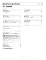
Data Sheet
Open the catalog to page 2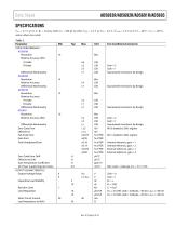
Data Sheet SPECIFICATIONS VDD = 2.7 V to 5.5 V, RL = 2 kΩ to GND, CL = 200 pF to GND, VREF = 2.5 V to VDD − 0.2 V, VLOGIC = 1.8 V to 5.5 V, −40°C < TA < +105°C, unless otherwise noted. Table 2. Parameter STATIC PERFORMANCE 1 AD5693R Resolution Relative Accuracy (INL) A Grade B Grade Differential Nonlinearity AD5692R Resolution Relative Accuracy Differential Nonlinearity AD5691R Resolution Relative Accuracy A Grade B Grade Differential Nonlinearity AD5693 Resolution Relative Accuracy (INL) Test Conditions/Comments Gain = 2 Gain = 1 Guaranteed monotonic by design Guaranteed monotonic by design...
Open the catalog to page 3
AD5693R/AD5692R/AD5691R/AD5693 Parameter REFERENCE OUTPUT Output Voltage Voltage Reference TC 3 A Grade B Grade Output Impedance Output Voltage Noise Output Voltage Noise Density Capacitive Load Stability Load Regulation Sourcing Load Regulation Sinking Output Current Load Capability Line Regulation Thermal Hysteresis Test Conditions/Comments At ambient temperature See the Terminology section ppm/°C ppm/°C Ω µV p-p nV/√Hz µF µV/mA µV/mA mA µV/V ppm ppm 0.1 Hz to 10 Hz At ambient temperature, f = 10 kHz, CL = 10 nF RL = 2 kΩ At ambient temperature, VDD ≥ 3 V At ambient temperature VDD ≥ 3 V At...
Open the catalog to page 4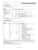
Data Sheet AC CHARACTERISTICS VDD = 2.7 V to 5.5 V, RL = 2 kΩ to GND, CL = 200 pF to GND, VREF = 2.5 V to VDD − 0.2 V, VLOGIC = 1.8 V to 5.5 V, −40°C < TA < +105°C, typical at 25°C, unless otherwise noted. Table 3. Parameter Output Voltage Settling Time 1, 2 Slew Rate Digital-to-Analog Glitch Impulse1 Digital Feedthrough1 Total Harmonic Distortion1 Output Noise Spectral Density1 Output Noise SNR SFDR SINAD 1 2 Conditions/Comments Gain = 1 ±1 LSB change around major carry, gain = 2 At ambient temperature, BW = 20 kHz, VDD = 5 V, fOUT = 1 kHz DAC code = midscale, 10 kHz 0.1 Hz to 10 Hz; internal...
Open the catalog to page 5
Data Sheet START OR REPEAT START CONDITION REPEAT START CONDITION STOP CONDITION Figure 3. I2C Serial Interface Timing Diagram STOP CONDITION LDAC ASYNCHRONOUS DAC UPDATE Figure 4. I2C RESET and LDAC Timing
Open the catalog to page 6
Stresses at or above those listed under Absolute Maximum Ratings may cause permanent damage to the product. This is a stress rating only; functional operation of the product at these or any other conditions above those indicated in the operational section of this specification is not implied. Operation beyond the maximum operating conditions for extended periods may affect product reliability. THERMAL RESISTANCE 0JA is defined by the JEDEC JESD51 standard, and the value is dependent on the test board and test environment. ' JEDEC 2S2P test board, still air (0 m/sec airflow). ESD (electrostatic...
Open the catalog to page 7All Analog Devices catalogs and technical brochures
 HMC722LP3E
8 Pages
 Isolated Sigma-Delta Modulator
17 Pages
 HMC853 Data Sheet
10 Pages
 AN-1084
8 Pages
 AN-1091
2 Pages
 AN_737
8 Pages
 AN-0982
4 Pages
 ADF7024
24 Pages
 AD9915
48 Pages
 AD9914
48 Pages
 ADRF6612
59 Pages
 ADRF6820
48 Pages
 ADL5246
32 Pages
 ADA4961
22 Pages
 AN-1141
8 Pages
 AN-698
36 Pages
 Temperature Sensors
2 Pages
 Reference Circuits
8 Pages
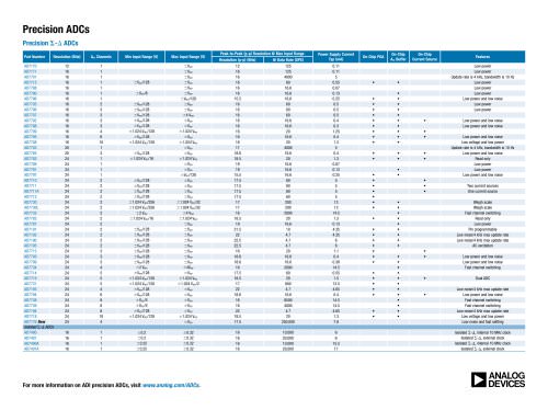
 Precision ADCs
16 Pages
 ADR02ACHIPS: ADR02ACHIPS
8 Pages
 AD9364 RF Agile Transceiver
32 Pages
 Digital Temperature Sensors
2 Pages
 Digital to Analog Converter ICs
12 Pages
 AD1836A: Multichannel 96 kHz Codec
24 Pages




























Archived catalogs
 Zero-Drift Amplifiers
2 Pages
 Powering ADI Components
8 Pages




- Ethernet switch
- Industrial network switch
- Acceleration sensor
- Unmanaged switch
- Analog Devices motor controller
- Transceiver module
- Triaxial acceleration sensor
- DC motor controller
- Analog Devices stepper motor controller
- Industrial converter
- Ethernet transceiver
- Processor
- High-voltage amplifier
- Low-noise amplifier
- Multiplexer
- Compact motor controller
- Digital converter
- Closed-loop motor controller
- Digital motor controller