- Catalogs
- Analog Devices
- AD5362/AD5363: 8-Channel, 16/14-Bit, Serial Input, Voltage-Output DAC Data Sheet (Rev. A)
AD5362/AD5363: 8-Channel, 16/14-Bit, Serial Input, Voltage-Output DAC Data Sheet (Rev. A)
1 /29Pages

AD5362/AD5363: 8-Channel, 16/14-Bit, Serial Input, Voltage-Output DAC Data Sheet (Rev. A)
1 /29Pages
Catalog excerpts
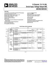
8-Channel, 16-/14-Bit, Serial Input, Voltage Output DAC AD5362/AD5363 FEATURES 8-channel DAC in 52-lead LQFP and 56-lead LFCSP packages Guaranteed monotonic to 16/14 bits Nominal output voltage range of −10 V to +10 V Multiple output voltage spans available Thermal shutdown function Channel monitoring multiplexer GPIO function System calibration function allowing user-programmable offset and gain Channel grouping and addressing features Data error checking feature SPI-compatible serial interface 2.5 V to 5.5 V digital interface Digital reset (RESET) Clear function to user-defined SIGGNDx Simultaneous update of DAC outputs APPLICATIONS Instrumentation Industrial control systems Level setting in automatic test equipment (ATE) Variable optical attenuators (VOA) Optical line cards FUNCTIONAL BLOCK DIAGRAM DVCC TEMP SENSOR CONTROL REGISTER GPIO REGISTER SERIAL INTERFACE X1 REGISTER M REGISTER C REGISTER X1 REGISTER M REGISTER C REGISTER AGND DGND X1 REGISTER M REGISTER C REGISTER OUTPUT BUFFER AND POWERDOWN CONTROL A/B SELECT 8 REGISTER X1 REGISTER BUFFER X2A REGISTER X2B REGISTER OUTPUT BUFFER AND POWERDOWN CONTROL · · · OUTPUT BUFFER AND POWERDOWN CONTROL OUTPUT BUFFER AND POWERDOWN CONTROL Rev. A Information furnished by Analog Devices is believed to be accurate and reliable. However, no responsibility is assumed by Analog Devices for its use, nor for any infringements of patents or other rights of third parties that may result from its use. Specifications subject to change without notice. No license is granted by implication or otherwise under any patent or patent rights of Analog Devices. Trademarks and registered trademarks are the property of their respective owners. One Technology Way, P.O. Box 9106, Norwood, MA 02062-9106, U.S.A. Tel: 781.329.4700 www.analog.com Fax: 781.461.3113 ©2008 Analog Devices, Inc. All rights reserved.
Open the catalog to page 1
Powered by TCPDF (www.tcpdf.org) IMPORTANT LINKS for the AD5362_5363* Last content update 09/06/2013 12:23 pm PARAMETRIC SELECTION TABLES Find Similar Products By Operating Parameters AD536x, AD537x Family Product Selection Guide Additional Similar Products DESIGN COLLABORATION COMMUNITY Collaborate Online with the ADI support team and other designers about select ADI products. Follow us on Twitter: www.twitter.com/ADI_News Like us on Facebook: www.facebook.com/AnalogDevicesInc DOCUMENTATION AN-0986: Adjusting the Output Range and Span of the AD5362 AN-1036: Clear to Any Voltage Using the AD5370...
Open the catalog to page 2
AD5362/AD5363 GENERAL DESCRIPTION The AD5362/AD5363 contain eight 16-/14-bit DACs in a single 52-lead LQFP package or 56-lead LFCSP package. The devices provide buffered voltage outputs with a span of 4× the reference voltage. The gain and offset of each DAC can be independently trimmed to remove errors. For even greater flexibility, the device is divided into two groups of four DACs, and the output range of each group can be independently adjusted by an offset DAC. The AD5362/AD5363 offer guaranteed operation over a wide supply range with VSS from −16.5 V to −4.5 V and VDD from 8 V to 16.5 V....
Open the catalog to page 4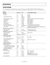
AD5362/AD5363 SPECIFICATIONS DVCC = 2.5 V to 5.5 V; VDD = 9 V to 16.5 V; VSS = −16.5 V to −4.5 V; VREF = 5 V; AGND = DGND = SIGGND0 = SIGGND1 = 0 V; RL = open circuit; gain (M), offset (C), and DAC offset registers at default values; all specifications TMIN to TMAX, unless otherwise noted. Table 2. Parameter ACCURACY Resolution Integral Nonlinearity (INL) Differential Nonlinearity (DNL) Zero-Scale Error Full-Scale Error Gain Error Zero-Scale Error 2 Full-Scale Error2 Span Error of Offset DAC VOUTx 3 Temperature Coefficient DC Crosstalk2 REFERENCE INPUTS (VREF0, VREF1)2 VREFx Input Current VREFx...
Open the catalog to page 5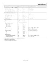
AD5362/AD5363 Parameter DIGITAL OUTPUTS (SDO, BUSY, GPIO, PEC) Output Low Voltage Output High Voltage (SDO) High Impedance Leakage Current High Impedance Output Capacitance2 TEMPERATURE SENSOR (TEMP_OUT)2 Accuracy Output Voltage at 25°C Output Voltage Scale Factor Output Load Current Power-On Time POWER REQUIREMENTS DVCC VDD VSS Power Supply Sensitivity2 ∆Full Scale/∆VDD ∆Full Scale/∆VSS ∆Full Scale/∆DVCC DICC IDD ISS Power-Down Mode DICC IDD ISS Power Dissipation Power Dissipation Unloaded (P) Junction Temperature 4 Test Conditions/Comments Sinking 200 μA Sourcing 200 μA SDO only V min/V max...
Open the catalog to page 6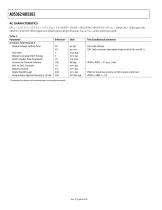
AD5362/AD5363 AC CHARACTERISTICS DVCC = 2.5 V; VDD = 15 V; VSS = −15 V; VREF = 5 V; AGND = DGND = SIGGND0 = SIGGND1 = 0 V; CL = 200 pF; RL = 10 kΩ; gain (M), offset (C), and DAC offset registers at default values; all specifications TMIN to TMAX, unless otherwise noted. Table 3. Parameter DYNAMIC PERFORMANCE1 Output Voltage Settling Time Slew Rate Digital-to-Analog Glitch Energy Glitch Impulse Peak Amplitude Channel-to-Channel Isolation DAC-to-DAC Crosstalk Digital Crosstalk Digital Feedthrough Output Noise Spectral Density @ 10 kHz 1 Test Conditions/Comments Full-scale change DAC latch contents...
Open the catalog to page 7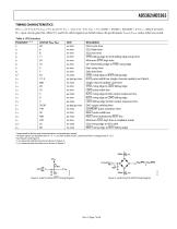
AD5362/AD5363 TIMING CHARACTERISTICS DVCC = 2.5 V to 5.5 V; VDD = 9 V to 16.5 V; VSS = −16.5 V to −8 V; VREF = 5 V; AGND = DGND = SIGGND = 0 V; CL = 200 pF to GND; RL = open circuit; gain (M), offset (C), and DAC offset registers at default values; all specifications TMIN to TMAX, unless otherwise noted. Table 4. SPI Interface Parameter 1, 2, 3 t1 t2 t3 t4 t5 t6 t7 t8 t9 4 t10 t11 t12 t13 t14 t15 t16 t17 t18 t19 t20 t21 t22 5 t23 Unit ns min ns min ns min ns min ns min ns min ns min ns min ns max μs typ/μs max ns max ns min ns min μs max ns min μs max μs typ/μs max ns max ns min μs max ns min...
Open the catalog to page 8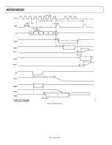
t23 1 LDAC ACTIVE DURING BUSY. 2 LDAC ACTIVE AFTER BUSY. Figure 4. SPI Write Timing
Open the catalog to page 9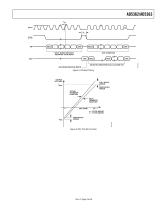
INPUT WORD SPECIFIES REGISTER TO BE READ DB0 SELECTED REGISTER DATA CLOCKED OUT LSB FROM PREVIOUS WRITE Figure 5. SPI Read Timing OUTPUT VOLTAGE FULL-SCALE ERROR + ZERO-SCALE ERROR ACTUAL TRANSFER FUNCTION IDEAL TRANSFER FUNCTION Figure 6. DAC Transfer Function
Open the catalog to page 10
ABSOLUTE MAXIMUM RATINGS TA = 25°C, unless otherwise noted. Transient currents of up to DVccto DGND Digital Inputs to DGND Digital Outputs to DGND Operating Temperature Range (TA) Storage Temperature Range Operating Junction Temperature Reflow Soldering Stresses above those listed under Absolute Maximum Ratings may cause permanent damage to the device. This is a stress rating only; functional operation of the device at these or any other conditions above those indicated in the operational section of this specification is not implied. Exposure to absolute maximum rating conditions for extended...
Open the catalog to page 11All Analog Devices catalogs and technical brochures
 HMC722LP3E
8 Pages
 Isolated Sigma-Delta Modulator
17 Pages
 HMC853 Data Sheet
10 Pages
 AN-1084
8 Pages
 AN-1091
2 Pages
 AN_737
8 Pages
 AN-0982
4 Pages
 ADF7024
24 Pages
 AD9915
48 Pages
 AD9914
48 Pages
 ADRF6612
59 Pages
 ADRF6820
48 Pages
 ADL5246
32 Pages
 ADA4961
22 Pages
 AN-1141
8 Pages
 AN-698
36 Pages
 Temperature Sensors
2 Pages
 Reference Circuits
8 Pages
 Precision ADCs
16 Pages
 ADR02ACHIPS: ADR02ACHIPS
8 Pages
 AD9364 RF Agile Transceiver
32 Pages
 Digital Temperature Sensors
2 Pages
 Digital to Analog Converter ICs
12 Pages
 AD1836A: Multichannel 96 kHz Codec
24 Pages


Archived catalogs
 Zero-Drift Amplifiers
2 Pages
 Powering ADI Components
8 Pages


- Ethernet switch
- Industrial network switch
- Acceleration sensor
- Unmanaged switch
- Transceiver module
- Analog Devices motor controller
- Triaxial acceleration sensor
- DC motor controller
- Data acquisition unit
- Analog Devices stepper motor controller
- Industrial converter
- Ethernet transceiver
- Processor
- High-voltage amplifier
- Low-noise amplifier
- Compact motor controller
- Gyroscope
- Closed-loop motor controller
- Digital converter