- Catalogs
- Analog Devices
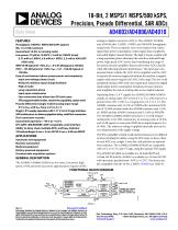
- AD4002/AD4006/AD4010: 18-Bit, 2 MSPS/1 MSPS/500 kSPS, Precision, Pseudo Differential, SAR ADCs Data Sheet (Rev. 0)
AD4002/AD4006/AD4010: 18-Bit, 2 MSPS/1 MSPS/500 kSPS, Precision, Pseudo Differential, SAR ADCs Data Sheet (Rev. 0)
1 /37Pages

AD4002/AD4006/AD4010: 18-Bit, 2 MSPS/1 MSPS/500 kSPS, Precision, Pseudo Differential, SAR ADCs Data Sheet (Rev. 0)
1 /37Pages
Catalog excerpts
18-Bit, 2 MSPS/1 MSPS/500 kSPS, Precision, Pseudo Differential, SAR ADCs AD4002/AD4006/AD4010 Data Sheet FEATURES analog-to-digital converters (ADCs). The AD4002, AD4006, and AD4010 offer 2 MSPS, 1 MSPS, and 500 kSPS throughputs, respectively. They incorporate ease of use features that reduce signal chain power consumption, reduce signal chain complexity, and enable higher channel density. The high-Z mode, coupled with a long acquisition phase, eliminates the need for a dedicated high power, high speed ADC driver, thus broadening the range of low power precision amplifiers that can drive these ADCs directly while still achieving optimum performance. The input span compression feature enables the ADC driver amplifier and the ADC to operate off common supply rails without the need for a negative supply while preserving the full ADC code range. The low serial peripheral interface (SPI) clock rate requirement reduces the digital input/output power consumption, broadens processor options, and simplifies the task of sending data across digital isolation. Throughput: 2 MSPS/1 MSPS/500 kSPS options INL: ±3.2 LSB maximum Guaranteed 18-bit, no missing codes Low power: 70 µW at 10 kSPS, 14 mW at 2 MSPS (total) 9.75 mW at 2 MSPS, 4.9 mW at 1 MSPS, 2.5 mW at 500 kSPS (VDD only) SNR: 95 dB typical at 1 kHz, VREF = 5 V; 95 dB typical at 100 kHz THD: −125 dB typical at 1 kHz, VREF = 5 V; −108 dB typical at 100 kHz Ease of use features reduce system power and complexity Input overvoltage clamp circuit Reduced nonlinear input charge kickback High-Z mode Long acquisition phase Input span compression Fast conversion time allows low SPI clock rates SPI-programmable modes, read/write capability, status word Pseudo differential (single-ended) analog input range 0 V to VREF with VREF from 2.4 V to 5.1 V Single 1.8 V supply operation with 1.71 V to 5.5 V logic interface SAR architecture: no latency/pipeline delay, valid first conversion First conversion accurate Guaranteed operation: −40°C to +125°C SPI-/QSPI-/MICROWIRE-/DSP-compatible serial interface Ability to daisy-chain multiple ADCs and busy indicator 10-lead packages: 3 mm × 3 mm LFCSP, 3 mm × 4.90 mm MSOP Operating from a 1.8 V supply, the AD4002/AD4006/AD4010 sample an analog input (IN+) from 0 V to VREF with respect to a ground sense (IN−) with VREF ranging from 2.4 V to 5.1 V. The AD4002 consumes only 14 mW at 2 MSPS with a minimum SCK rate of 75 MHz in turbo mode; the AD4006 consumes only 7 mW at 1 MSPS; and the AD4010 consumes only 3.5 mW at 500 kSPS. The AD4002/AD4006/AD4010 all achieve ±3.2 LSB integral nonlinearity error (INL) maximum, no missing codes at 18 bits, and 95 dB signal-to-noise ratio (SNR) for an input frequency (fIN) of 1 kHz. The reference voltage is applied externally and can be set independently of the supply voltage. The SPI-compatible versatile serial interface features seven different modes including the ability, using the SDI input, to daisy-chain several ADCs on a single 3-wire bus, and provides an optional busy indicator. The AD4002/AD4006/AD4010 are compatible with 1.8 V, 2.5 V, 3 V, and 5 V logic, using the separate VIO supply. APPLICATIONS Automatic test equipment Machine automation Medical equipment Battery-powered equipment Precision data acquisition systems The AD4002/AD4006 are available in a 10-lead MSOP and 10-lead LFCSP, and the AD4010 is available in a 10-lead LFCSP, with operation specified from −40°C to +125°C. The devices are pin compatible with the 18-bit, 2 MSPS AD4003 (see Table 8). GENERAL DESCRIPTION The AD4002/AD4006/AD4010 are low noise, low power, high speed, 18-bit, precision successive approximation register (SAR) FUNCTIONAL BLOCK DIAGRAM 2.4V TO 5.1V 10µF HIGH-Z MODE TURBO MODE SERIAL INTERFACE STATUS BITS 3-WIRE OR 4-WIRE SPI INTERFACE (DAISY CHAIN, CS) 16233-001 Document Feedback Information furnished by Analog Devices is believed to be accurate and reliable. However, no responsibility is assumed by Analog Devices for its use, nor for any infringements of patents or other rights of third parties that may result from its use. Specifications subject to change without notice. No license is granted by implication or otherwise under any patent or patent rights of Analog Devices. Trademarks and registered trademarks are the property of their respective owners. One Technology Way, P.O. Box 9106, Norwood, MA 02062-9106, U.S.A. Tel: 781.329.4700 ©2018 Analog Devices, Inc. All rights reserved. Technical Su
Open the catalog to page 1
Data Sheet REVISION HISTORY 1/2018—Revision 0: Initial Version
Open the catalog to page 2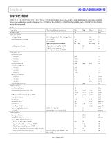
AD4002/AD4006/AD4010 SPECIFICATIONS VDD = 1.71 V to 1.89 V, VIO = 1.71 V to 5.5 V, Vref = 5 V, all specifications Tmin to Tmax, high-Z mode disabled, span compression disabled, turbo mode enabled, and sampling frequency (fS) = 2 MSPS for the AD4002, fS = 1 MSPS for the AD4006, and fS = 500 kSPS for the AD4010, unless otherwise noted. Test Conditions/Comments Unit Bits ANALOG INPUT Voltage Range Operating Input Voltage Analog Input Current IN+ Voltage (Vin+) - IN- Voltage (Vin-) Vin+ to GND Vin- to GND Span compression enabled Acquisition phase, Ta = 25°C High-Z mode enabled, converting dc input...
Open the catalog to page 3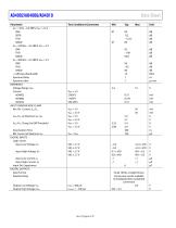
Data Sheet
Open the catalog to page 4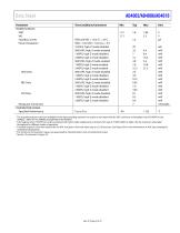
1 The acquisition phase is the time available for the input sampling capacitors to acquire a new input with the ADC running at a throughput rate of 2 MSPS for the AD4002, 1 MSPS for the AD4006, and 500 kSPS for the AD4010. 2 A throughput rate of 2 MSPS can only be achieved with turbo mode enabled and a minimum SCK rate of 75 MHz. Refer to Table 4 for the maximum achievable throughput for different modes of operation. 3 Transient response is the time required for the ADC to acquire a full-scale input step to ±2 LSB accuracy. See Figure 39 for more information on ADC input settling for multiplexed...
Open the catalog to page 5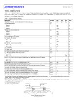
Data Sheet AD4002/AD4006/AD4010 TIMING SPECIFICATIONS VDD = 1.71 V to 1.89 V, VIO = 1.71 V to 5.5 V, Vref = 5 V, all specifications Tmin to Tmax, high-Z mode disabled, span compression disabled, turbo mode enabled, and fS = 2 MSPS for the AD4002, fS = 1 MSPS for the AD4006, and fS = 500 kSPS for the AD4010, unless otherwise noted. See Figure 2 for the timing voltage levels. Table 2. Digital Interface Timing 1FOR VIO < 2.7V, X = 80, AND Y = 20; FOR VIO > 2.7V, X = 70, AND Y = 30. 2MINIMUM VIH AND MAXIMUM VIL USED. SEE DIGITAL INPUTS SPECIFICATIONS IN TABLE 1. Figure 2. Voltage Levels for Timing...
Open the catalog to page 6All Analog Devices catalogs and technical brochures
 HMC722LP3E
8 Pages
 Isolated Sigma-Delta Modulator
17 Pages
 HMC853 Data Sheet
10 Pages
 AN-1084
8 Pages
 AN-1091
2 Pages
 AN_737
8 Pages
 AN-0982
4 Pages
 ADF7024
24 Pages
 AD9915
48 Pages
 AD9914
48 Pages
 ADRF6612
59 Pages
 ADRF6820
48 Pages
 ADL5246
32 Pages
 ADA4961
22 Pages
 AN-1141
8 Pages
 AN-698
36 Pages
 Temperature Sensors
2 Pages
 Reference Circuits
8 Pages
 Precision ADCs
16 Pages
 ADR02ACHIPS: ADR02ACHIPS
8 Pages
 AD9364 RF Agile Transceiver
32 Pages
 Digital Temperature Sensors
2 Pages
 Digital to Analog Converter ICs
12 Pages
 AD1836A: Multichannel 96 kHz Codec
24 Pages


Archived catalogs
 Zero-Drift Amplifiers
2 Pages
 Powering ADI Components
8 Pages


- Ethernet switch
- Industrial network switch
- Acceleration sensor
- Unmanaged switch
- Transceiver module
- Analog Devices motor controller
- Triaxial acceleration sensor
- DC motor controller
- Analog Devices stepper motor controller
- Industrial converter
- Ethernet transceiver
- High-voltage amplifier
- Low-noise amplifier
- Multiplexer
- Compact motor controller
- Gyroscope
- Closed-loop motor controller