- Catalogs
- Analog Devices
- AN_737
AN_737
1 /8Pages

AN_737
1 /8Pages
Catalog excerpts

AN-737 APPLICATION NOTE One Technology Way • P.O. Box 9106 • Norwood, MA 02062-9106, U.S.A. • Tel: 781.329.4700 • Fax: 781.461.3113 • www.analog.com How ADIsimADC Models an ADC by Brad Brannon and Tom MacLeod CONVERTER MODELING Converter modeling has often been overlooked, omitted, or accomplished using an ideal data converter model. With more and more systems using mixed-signal technology, the importance of system modeling is ever increasing. Coupled with shortened design cycles and pressure for first pass success, this drives the continuing importance of complete system modeling. ADIsimADC™ has been developed to answer this growing need. Often ideal converter models are used for functional modeling, but these fail to give the required details of performance to determine if a particular device meets the desired goals of the system. This is why ADIsimADC has been developed. For the first time, ADIsimADC provides a means for users to validate performance of a particular converter in their system, using their conditions to determine the applicability of a selected device. While ADIsimADC does not emulate every characteristic of an ADC, it goes a long way towards achieving the goal of allowing users to model real converters in their system simulations. BIT EXACT vs. BEHAVIORAL A bit exact model is a model that, given a known stimulus, provides a known and predictable output. ADIsimADC is not a bit exact model. These types of models are often found in digital systems. In dealing with analog functions, there is never a known response for a given input because of noise, distortion, and other nonlinearities. While some portion of the response may be predictable, much of the remainder is subject to distortion, noise, and even part-to-part variation. Additionally, to provide a bit exact model requires providing circuit simulation files, such as SPICE models, that process transient response. However, these models are large, complex, very slow and, in the end, provide limited accuracy. A reduced or equivalent SPICE model reduces the complexity, but is not able to provide adequate modeling of fine details of static and dynamic performance. A behavior model eliminates the complexity and, at the same time, allows modeling of fine performance details not possible to attain with a circuit file. ADIsimADC in conjunction with VisualAnalog™ acts as a standalone converter evaluation tool. ADIsimADC™ can also be used with many other third party simulation tools, including ADS from Agilent Technologies, VSS from Applied Wave Research, Inc, National Instrument tools, as well as MATLAB® and C++. Usage information with these tools can be found at www.analog.com/ADIsimADC. MODEL vs. HARDWARE Modeling a system or an ADC should never be a substitute for building and characterizing a real system. It is one thing to model a circuit, but it is another matter to actually build it and test it. As with any analog or mixed-signal device, proper layout and configuration is required to achieve the performance shown in simulation. Therefore, it is important that all layout rules and guidelines be followed as shown in the product data sheet (see Figure 4). An example is the importance of providing adequate power supply bypass capacitors. Because mixed-signal devices include some amount of digital circuitry, digital switching noise is often a problem, and failure to provide capacitors to moderate these switching currents can significantly reduce performance of even the best devices. Other support devices are often required around the converter, including additional capacitors, inductors, and resistors. The best way to know what is required is to consult the product data sheet and the evaluation board schematic. WHICH SPECIFICATIONS ARE IMPORTANT TO MODEL? ADIsimADC is targeted to provide realistic performance of real devices. Which specification is important to model depends on what kind of analysis the user is trying to perform. For example, control loops need accurate transfer function and delay information, while radio systems may require an accurate representation of noise and distortion. ADIsimADC models many of the critical specifications of data converters, including: offset, gain, sample rate, bandwidth, jitter, latency, and both ac and dc linearity. (See the AN-835 Application Note Understanding High Speed ADC Testing and Evaluation, for additional information on ac linearity.) This application note describes these specifications in detail and how ADIsimADC treats them.
Open the catalog to page 1
Application Note
Open the catalog to page 2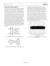
Application Note GAIN, OFFSET, AND DC LINEARITY The full-scale range of the converter is defined by the design of the converter. It can be fixed, selectable, or variable. Gain error of a converter is the deviation from the nominal value, often called the input span. Because an ADC is a voltage input device, the full-scale range is specified in volts at dc or low frequency. Offset is defined as the deviation of the actual major carrier transition from one-half of the full-scale range of the converter. This can be measured by shorting the input(s) to one-half of the full scale. Many devices have...
Open the catalog to page 3
Figure 4. Typical Evaluation Board Schematic: Shows Typical Support Components 3. AC-COUPLED ENCODE IS STANDARD. C5, C6, C33, C34, R1, R11−R14 AND U8 ARE NOT INSTALLED. IF PECL ENCODE IS REQUIRED, CR1 AND T2 ARE NOT INSTALLED. 2. AC-COUPLED AIN IS STANDARD, R3, R4, R5, R8 AND U3 ARE NOT INSTALLED. IF DC-COUPLED AIN IS REQUIRED, C30, R15 AND T3 ARE NOT INSTALLED. 1. R2 IS INSTALLED FOR INPUT MATCHING ON THE PRIMARY OF T3. R15 IS NOT INSTALLED. R15 IS INSTALLED FOR INPUT MATCHING ON THE SECONDARY OF T3, R2 IS NOT INSTALLED. INSTALL JUMPER DC-COUPLED AIN OPTION (SEE NOTE 2) DO NOT INSTALL DC-COUPLED...
Open the catalog to page 4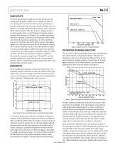
Application Note SAMPLE RATE DISTORTION: DYNAMIC AND STATIC Due to an ADC’s finite bandwidth, there is also a fundamental slew rate limitation, or dynamic limitation. This slew rate limitation is one source of distortion within an ADC. As the input frequency of a data converter is swept from dc to some upper frequency, the SFDR performance and the harmonic performance of the converter decline (see Figure 7). 100 95 WORST OTHER SPUR HARMONICS (SECOND, THIRD) Figure 7. Typical Converter Performance vs. Analog Input Frequency Figure 6. Typical Converter Analog Bandwidth ENOB (BITS), –20dB INPUT...
Open the catalog to page 5All Analog Devices catalogs and technical brochures
 HMC722LP3E
8 Pages
 Isolated Sigma-Delta Modulator
17 Pages
 HMC853 Data Sheet
10 Pages
 AN-1084
8 Pages
 AN-1091
2 Pages
 AN-0982
4 Pages
 ADF7024
24 Pages
 AD9915
48 Pages
 AD9914
48 Pages
 ADRF6612
59 Pages
 ADRF6820
48 Pages
 ADL5246
32 Pages
 ADA4961
22 Pages
 AN-1141
8 Pages
 AN-698
36 Pages
 Temperature Sensors
2 Pages
 Reference Circuits
8 Pages
 Precision ADCs
16 Pages
 ADR02ACHIPS: ADR02ACHIPS
8 Pages
 AD9364 RF Agile Transceiver
32 Pages
 Digital Temperature Sensors
2 Pages
 Digital to Analog Converter ICs
12 Pages
 AD1836A: Multichannel 96 kHz Codec
24 Pages


Archived catalogs
 Zero-Drift Amplifiers
2 Pages
 Powering ADI Components
8 Pages


- Ethernet switch
- Industrial network switch
- Acceleration sensor
- Unmanaged switch
- Transceiver module
- Analog Devices motor controller
- Triaxial acceleration sensor
- DC motor controller
- Data acquisition unit
- Analog Devices stepper motor controller
- Industrial converter
- Ethernet transceiver
- Processor
- High-voltage amplifier
- Low-noise amplifier
- Multiplexer
- Compact motor controller
- Gyroscope
- Closed-loop motor controller
- Digital converter