


- Products
- Catalogs
- News & Trends
- Exhibitions
CMV50000

CMV50000
The CMV50000 is a high-speed CMOS image sensor with a 47.5MP resolution, designed for machine vision and video applications. It features a global shutter pixel array, programmable analog gain amplifier, and offset regulation. The sensor supports a frame rate of 30 fps at full resolution, with higher rates possible through programmable modes. It includes a dual exposure HDR mode for extended dynamic range.
- High resolution of 7920x6004 pixels
- 8T global shutter pixel with true Correlated Double Sampling
- Low noise and high sensitivity for low light conditions
- Full well capacity of 58000e- in binning mode
- 35mm Full Frame optical format
- On-chip digital sequencer for easy operation
- Machine vision
- Video/Broadcast
- Security
- High-end inspection
- Aerial mapping
- Document scanning
- Intelligent Transportation Systems (ITS)
- Scientific and 3D imaging
Available in mono and color options, with or without window, in trays of 10 pieces.
The datasheet provides a detailed pin diagram and description, including digital inputs, analog supplies, and sub-LVDS channel outputs.
Includes electrical parameters, electrostatic discharge ratings, and temperature ranges. Operating junction temperature ranges from -30°C to 70°C.
Details power supply requirements, digital I/O specifications, and sub-LVDS interface characteristics. Total power consumption is 2.5W idle and 3.0W running.
Includes electro-optical characteristics, highlighting typical values across the operating temperature range.
The CMV50000 sensor features an effective pixel resolution of 7920 × 6004 with a pixel pitch of 4.6 × 4.6 µm², suitable for a 35mm full-frame optical format. It employs a global shutter with true correlated double sampling (CDS) for noise correction. The sensor supports a pipelined global shutter, allowing exposure of the next image during the readout of the previous one. It offers a full well charge of 14500 e- in normal mode and 58000 e- in binning mode, with conversion gains of 0.27 DN/e- and 0.068 DN/e- respectively. The dynamic range is 64 dB in normal mode and 68 dB in binning mode, with a maximum signal-to-noise ratio (SNRMAX) of 41.6 dB and 47.6 dB respectively.
The sensor requires six external power supplies, with a distinction between digital and analog supplies. Proper decoupling and grounding are essential to minimize noise. The power-up sequence involves a specific order and timing to avoid peak currents and ensure proper initialization. The sensor's operation is controlled via an SPI interface, which configures settings such as windowing, subsampling, gain, and offset.
It is recommended to separate analog and digital ground nets and connect them close to the external supply regulators for optimal noise performance. The sensor includes on-chip regulators for biasing, which require external connections on the PCB level. Capacitors of specific types and values are necessary for decoupling the supply regulators.
The sensor architecture includes an active pixel array driven by row logic and drivers, with data readout via an analog front-end, ADC, and digital post-processing block. The sensor outputs data through 22 sub-LVDS channels, with an on-chip sequencer managing control signals. The pixel array consists of effective, optical black, and buffer pixels, with micro-lenses to enhance quantum efficiency.
The spectral characteristics and responsivity graphs indicate the sensor's performance across different wavelengths, with quantum efficiency and responsivity varying for mono and color devices. The power supply diagrams illustrate the necessary decoupling and grounding configurations.
The SPI interface is crucial for configuring the sensor, with SPI_CLK being a part of this interface. The sensor operates as an SPI slave, and the interface consists of four wires: SPI_CSN, SPI_CLK, SPI_MOSI, and SPI_MISO. Data is transferred between the master and slave using these wires, with specific sequences for read and write operations. The SPI_CSN is an active-low chip select, and the SPI_CLK is rising-edge triggered. Multiple sensors can share SPI_CLK and SPI_MOSI, with SPI_CSN acting as a chip select for each slave.
The sensor's configuration registers are organized into four banks, each containing 127 8-bit registers. The BANK_SEL register at address 0 is used to select the active register bank. Registers are categorized based on when they can be updated, such as SYNC, FRAME, DC, RST, and RO categories. SYNC registers are synchronized to the start of a frame, while FRAME registers control frame and exposure timing.
The sensor features both a hard reset (RST_N) and a soft reset (CMD_RST_SOFT_N), both active-low. The soft reset affects the entire sensor except the SPI interface and register bank, allowing for retention of register values during a reset.
The sensor operates in various states: RESET, IDLE, EXPOSURE, GLOB, and READOUT. Sequential operation involves a cycle of EXPOSURE, GLOB, and READOUT, returning to IDLE after completion. Pipelined operation allows EXPOSURE and READOUT to overlap, enabling continuous frame capture. Shutter lag is present by default, causing a delay between the EXPOSURE state and actual exposure. This can be disabled by setting the NO_SHUTTER_LAG register high, aligning the start of actual exposure with the EXPOSURE state.
The document describes various control modes for sensor operation, each with distinct characteristics and dependencies on external inputs and register configurations. The control modes are set using the CTRL_MODE register.
This mode allows full control of exposure timing via sensor input pins. Key transitions include moving to the EXPOSURE state with a rising edge on REQ_EXP and to the GLOB state with REQ_FRAME. The timing between these triggers defines the exposure length. Invalid timings can disrupt operations, leading to corrupted data.
Similar to Full External, but the transition from EXPOSURE to GLOB is controlled by a programmable time set in the register, not by REQ_FRAME. Invalid and special timing conditions are similar to Full External mode.
This mode allows a single request to trigger a sequence of frames at a programmable frame rate. The mode is internally controlled, and invalid register settings can affect operation. Special timing conditions include extending sequence length with new requests.
Streaming mode is an extension of Triggered Internal mode with an infinite sequence length, continuously generating frames until stopped. There are no invalid or special control timings once started.
Triggered Internal mode is more forgiving, adjusting timing to ensure complete images, while Programmed and Full External modes respond directly to external requests, risking image corruption but ensuring no missed exposures. Streaming mode provides continuous operation.
The document outlines several software command registers for controlling sensor operations. These include CMD_RST_SOFT_N, CMD_REQ_EXP, CMD_REQ_FRAME, CMD_HALT_BLOCK, and CMD_HALT_NBLOCK. The CMD_REQ_EXP and CMD_REQ_FRAME registers are equivalent to their sensor input counterparts, allowing for frame timing control via register uploads. The HALT commands are used to stop sensor operations, with CMD_HALT_BLOCK completing the active READOUT before moving to IDLE, and CMD_HALT_NBLOCK immediately stopping all operations.
The CMV50000 sensor uses sub-LVDS outputs to transport image data, consisting of 26 output pairs for data, OB data, control, and clock channels. The data channels transfer pixel data, while the control channel provides status information. The output clock channel is used for data sampling, operating at half the output data rate. The document describes two readout formats: pixel-based and packet-based.
This format aligns data in pixels using a side-band control channel. Data is transferred serially, LSB first, with all channels word-aligned. The control channel transmits status information in a word-based format, with bits indicating data validity and sensor states.
Data can be formatted in byte-aligned packets, consisting of SYNC, HEADER, PAYLOAD, optional padding, and CRC. The CTR_OUT channel sends meta-data packets, while DATAx_OUT and OBx_OUT channels send pixel data packets during READOUT. The HEADER code provides packet information, and the CRC ensures data integrity.
The document provides guidance on configuring the sensor for different operation modes, with details on exposure control and image readout provided in subsequent sections.
The document outlines various data multiplexing modes, ranging from using all 22 output channels to a single output channel. Each mode is designated as MUX.1 to MUX.9, allowing for flexibility in data handling based on the number of channels utilized.
Four sensor control modes are described: Full External, Programmed External, Triggered Internal, and Streaming. These modes provide different levels of control over the sensor's operation.
The document specifies image modes for both color and monochrome outputs, including full array readout, sub-sampling, and binning options.
Three analog gain modes are available: ×1, ×2, and ×4, allowing for adjustments in signal amplification.
Optical black clamping can be toggled on or off, affecting the sensor's handling of black levels.
A flow chart is provided to guide the configuration or reconfiguration of the sensor, detailing both static and dynamic parts of the process. It emphasizes the importance of following the recommended order to avoid unpredictable sensor behavior.
The power-up and power-down sequences are crucial for proper sensor operation, with specific steps outlined for each.
A sequence of SPI data writes is necessary for sensor operation, with specific values provided for each register.
The document details the register settings required to configure the sensor's output format and PLL, including calculations for parameters like pll1_pre_div and pll1_ndiv based on input clock frequency and desired data rate.
Equations are provided to calculate necessary adjustments to shutter timing parameters to maintain consistent pixel array timing.
Procedures for enabling on-chip regulators and internal biases are outlined, including specific register values and settling times.
Register settings for different image and gain modes are provided, with adjustments based on the selected mode.
The document discusses the offset in optical black (OB) pixels compared to effective pixels in dark conditions. The EOB_OFFSET_FINE register is used to compensate for this offset, with specific settings depending on the analog gain mode. The OB correction requires specific uploads per OB clamping mode, detailed in section 7.7.1.
Section 7.5.1 outlines the configuration of frame and exposure times using various registers. The sensor control modes dictate how frame and exposure times are set, either externally or via registers. The TIME_UNIT register defines the unit for these times, with a nominal CLK_PIX frequency of 69.167 MHz. Default settings provide a frame time of 50 ms and an exposure time of 10 ms.
The document describes a dual exposure mode allowing two different exposure times within one image, enhancing HDR capabilities. The DUAL_EXPOSURE and DUAL_EXP_GROUPING registers control this feature, with specific configurations for monochrome and color sensors.
Frame time must meet a minimum requirement to ensure successful frame readout and exposure. The document provides an equation to calculate this minimum frame time, considering various components like Tglob and Tread.
The maximum frame rate is achieved when frame time is minimized, and exposure time is less than readout time. The document provides equations to calculate the frame rate and the components involved.
In triggered internal mode, the NROF_FRAMES register determines the sequence length of frames captured. The ROW_LENGTH register defines the DVAL frequency during readout, with constraints based on the number of outputs and readout mode.
The sensor supports multiple vertical windows for regions of interest (ROI), with configurations for position, size, and subsampling. The YWIN_ENA register enables these windows, and the YWINi.SUBS register defines vertical subsampling ratios.
The document briefly mentions horizontal subsampling settings controlled by the XSUBS register, with ratios defined by the register value.
The sensor supports horizontal subsampling, reducing pixels per line to 1:2XSUBS, applied to the whole array. In color mode, pixel grouping preserves the Bayer pattern, while in monochrome mode, only 1 out of 2x2 neighboring pixels is read. Combining horizontal and vertical subsampling halves the image resolution in both dimensions.
The sensor supports color and monochrome binning modes, summing values of 4 pixels before ADC, reducing resolution by x4 but increasing full well charge, dynamic range, and SNR. In color mode, the Bayer pattern is preserved. Binning mode cannot be combined with horizontal subsampling, and XSUBS must be set to 0 when binning is enabled.
The output format can be selected using the OUTP_FORMAT register, with options for pixel-based or packet-based formats. Word alignment varies based on the format, with pixel-based alignment using a training word and packet-based alignment using a fixed SYNC code.
The sensor has 22 output channels, allowing for simultaneous output of 22 pixels. The number of channels used can be programmed to save power, with options for distributing channels evenly or using the first N channels.
Optical Black Clamping (OBC) can be enabled or bypassed. When enabled, it automatically corrects black levels based on OB pixels. Analog and digital gains can be adjusted, with digital gain specified for individual color channels.
The document describes digital gain registers for even and odd rows and columns. It is recommended to use analog gain over digital gain for better signal-to-noise ratio (SNR).
The COLOR_MODE register determines sensor mode: 0 for monochrome and 1 for color. Subsampling and binning modes differ based on this setting.
- Digital Test Output: Allows real-time monitoring of digital signals via the TDIGO1 pin, useful for testing and debugging.
- OTP Memory: Contains device serial number and temperature data from wafer tests. Accessible via SPI interface.
- Temperature Sensor: Provides temperature readings with varying accuracy based on calibration. Procedures for no calibration, 1-point, and 2-point calibration are detailed.
- Version ID: A read-only register that contains the sensor's revision number.
- Enable Optical Black Outputs: Describes the SPI sequence to enable or disable OB channels.
- Test Images: Test patterns can replace data streams for debugging. Modes include gradient and pseudo-random generator outputs.
Provides an overview of various registers, including their addresses and functions, such as PARAM_HOLD, COLOR_MODE, and others related to frame synchronization and exposure settings.
The document is a technical datasheet for the CMV50000, detailing the register descriptions and configurations for the device. It includes information on various registers, their addresses, bit names, default values, access types, and descriptions of their functions.
- Register Overview: This section provides a comprehensive list of registers, categorized into different banks. Each register is identified by an address and a name, with reserved spaces indicated where applicable.
- Detailed Register Descriptions: This section elaborates on specific registers, providing detailed information on each bit within the register, including its name, default value, access type, and a description of its function. Key registers include:
- BANK_SEL Register: Allows selection of different banks (0 to 3).
- PARAM_HOLD Register: Controls frame synchronization during SPI upload.
- DISABLE_FRAMESYNC Register: Enables or disables frame synchronization.
- CMD_REGS Register: Contains commands for soft reset, exposure state, and sensor states.
- COLOR_MODE Register: Switches between monochrome and color modes.
- OUTP_FORMAT Register: Sets the output format to pixel-based or packet-based.
- CTRL_MODE Register: Defines the control mode of the sensor, such as Full External, Programmed External, Triggered Internal, or Streaming.
- TIME_UNIT Register: Sets the unit for frame and exposure time.
- DUAL_EXPOSURE Register: Enables or disables dual exposure HDR.
- YWIN Registers: Define window sizes, start addresses, and subsampling ratios for different windows (YWIN0 to YWIN9).
- GDIG Registers: Set digital gains for pixels in various row and column configurations.
- EOB_TARGET Register: Sets the target black level value.
- GANA Register: Configures the analog gain for non-binning and binning modes.
- TRAINING_WORD Register: Specifies the training word on data outputs.
- TEST_LVDS Register: Sets the output test mode, including normal data output and test images.
- Frame and Exposure Time: Configured through TIME_UNIT and FRAME_TIME registers.
- Window Configuration: Managed through YWIN registers, allowing customization of window size, start position, and subsampling.
- Gain Settings: Digital and analog gains are adjustable via GDIG and GANA registers, respectively.
- Output Format and Control: Defined by OUTP_FORMAT and CTRL_MODE registers, providing flexibility in data output and sensor control.
The datasheet provides a detailed guide for configuring and utilizing the CMV50000's registers, offering flexibility in sensor operation and data management. It is essential for users to understand each register's function and configuration to optimize the device's performance.
The document outlines compliance with the EU 2015/863 amendment, which includes restrictions on six substance categories and an additional four. Specifically, lead content must not exceed 0.1% by weight in homogeneous materials. Products designed for high-temperature soldering are suitable for lead-free processes.
In addition to RoHS compliance, ams Green products are free from Bromine (Br) and Antimony (Sb) based flame retardants, with neither exceeding 0.1% by weight in homogeneous materials. Chlorine content is also restricted to 0.1% by weight.
The information reflects ams AG's knowledge as of the document's date, based on third-party data. While efforts are made to ensure accuracy, ams AG does not guarantee the information's precision and may not have conducted chemical analyses. Some proprietary information, such as CAS numbers, may not be disclosed.
ams AG is headquartered in Premstaetten, Austria. Contact details, including phone numbers and websites for product purchases, technical support, and feedback, are provided. For further inquiries, email [email protected].
Catalog excerpts

CMV50000 47.5MP CMOS Machine Vision Image Sensor
Open the catalog to page 1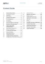
Document Feedback Content Guide 7.7 Configuring the On-Chip Data Processing . 89 10 Package Drawings & Markings. 132
Open the catalog to page 2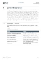
Document Feedback General Description The CMV50000 is a high speed CMOS image sensor with 7920 × 6004 effective pixels (47.5Mp) developed for machine vision and video applications. The image array consists of 4.6µm pipelined 8T global shutter pixels which allow exposure during read out, while performing true CDS (Correlated Double Sampling) operation. The image sensor also integrates a programmable analog gain amplifier and offset regulation. The image sensor has 22 digital sub-LVDS data output channels. Each output channel runs up to 830 Mbit/s, which results in a frame rate of 30 fps at full...
Open the catalog to page 3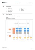
Document Feedback Machine vision Video/Broadcast Security High-end inspection Aerial mapping Document scanning ITS Scientific 3D imaging Block Diagram The functional blocks of this device are shown below: Figure 2 : Functional Blocks of CMV50000 Pixel array 7920 x 6004 (effective) active pixels CTR_OUT channel OBR_OUT channel CLK_OUT channel Digital sequencer
Open the catalog to page 4
Document Feedback 2 Ordering Information Ordering Code Package Chroma Options Delivery Quantity CMV50000-1E3M1PN PGA Mono windowless 10 Pcs / Tray
Open the catalog to page 5
Document Feedback 3 Pin Assignment 3.1 Pin Diagram Figure 3 : Pin Numbering (bottom view) 3.2 Pin Description Figure 4: Pin Description of CMV50000
Open the catalog to page 6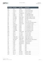
Document Feedback
Open the catalog to page 7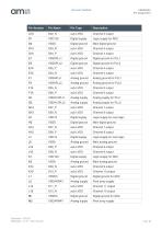
Document Feedback
Open the catalog to page 8
Document Feedback
Open the catalog to page 9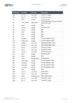
Document Feedback
Open the catalog to page 10
Document Feedback CMV50000 Absolute Maximum Ratings Absolute Maximum Ratings Stresses beyond those listed under “Absolute Maximum Ratings” may cause permanent damage to the device. These are stress ratings only. Functional operation of the device at these or any other conditions beyond those indicated under “Operating Conditions” is not implied. Exposure to absolute maximum rating conditions for extended periods may affect device reliability. Figure 5: Absolute Maximum Ratings of CMV50000 Symbol Electrical Parameters ISCR Input Current (latch-up immunity) Electrostatic Discharge ESDHBM Temperature...
Open the catalog to page 11
Document Feedback 5 Electrical Characteristics All limits are guaranteed. The parameters with Min and Max values are guaranteed with production tests or SQC (Statistical Quality Control) methods. Figure 6: Electrical Characteristics of CMV50000 Symbol Parameter Power Supplies Logic Supply Voltage of digital core, PLL Logic Supply Voltage of ADC I/O Supply Voltage for sub-LVDS, CMOS I/O's VDD27 Main Analog Supply Voltage; Supply Voltage for negative regulators VDDARRAY Pixel Array Supply Voltage VDD33 Internal Regulator Supply Voltage IDDARRAY Supply Current Ptot Total Power Consumption Idle Running...
Open the catalog to page 12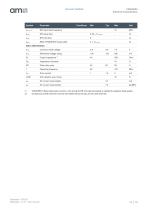
Symbol Parameter Electrical Characteristics fSPI_CLK SPI input clock frequency tsetup SPI setup time thdd SPI hold time tREQ REQ_FRAME/EXP pulse width VCM Common mode voltage VOD Differential voltage swing DC Clock duty cycle AIOD IOD variation over Temp. (1) VDDARRAY draws high peak currents (>1 A) during GLOB. Enough decoupling is needed to suppress these peaks. (2) Unused sub-LVDS channels must be terminated the same way as the used channels.
Open the catalog to page 13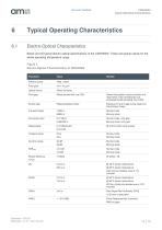
Document Feedback CMV50000 Typical Operating Characteristics 6 Typical Operating Characteristics 6.1 Electro-Optical Characteristics Below are the typical electro-optical specifications of the CMV50000. These are typical values for the whole operating temperature range. Figure 7: Electro-Optical Characteristics of CMV50000 Parameter Value Optical format 35mm full frame Pixel type Global shutter with true CDS Shutter type Pipelined global shutter Full well charge 14500 e- Allows fixed pattern noise correction and reset (kTC) noise canceling by true correlated double sampling (true-CDS). Exposure...
Open the catalog to page 14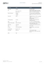
Document Feedback
Open the catalog to page 15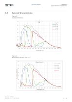
Document Feedback CMV50000 Typical Operating Characteristics 6.2 Spectral Characteristics Figure 8 : Quantum Efficiency
Open the catalog to page 16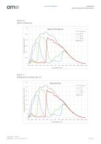
Typical Operating Characteristics Figure 11 : Responsivity (Analog Gain x4)
Open the catalog to page 17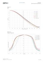
Typical Operating Characteristics Figure 13 : Angular Response
Open the catalog to page 18
Document Feedback Functional Description Sensor Architecture Figure 2 shows a high-level representation of the chip architecture for the CMV50000 sensor. The drawing shows the active pixel array and the periphery around it that enables the control and readout of the pixels. The core of the image sensor is made up from the pixel array, which is driven from two sides by 2 instances of the row logic and drivers. The pixel control signals are created globally by the global drivers and distributed to the sides of the sensor. The pixel data is read out row by row using a data path consisting of an...
Open the catalog to page 19
Document Feedback Figure 14: Pixel Array Buffer Pixels Black Columns Black Columns Buffer Pixels Buffer Pixels Effective Pixels Buffer Pixels Effective OB 7920 (effective) 22 buffer pixels 98 OB pixels (68 eff. OB) 22 buffer pixels 98 OB pixels (68 eff. OB) 8160 The pixel array can be split up in 3 parts: Optical black (OB) pixels (left and right side), buffer pixels (around effective array perimeter) and effective pixels. Only the 68 effective OB pixels are used for internal row clamping, which improves row noise and allows setting a pre-defined black level. The buffer pixels form a guard ring...
Open the catalog to page 20
Document Feedback
Open the catalog to page 21
Document Feedback The 3 main internal clocks are CLK_ADC, CLK_SER and CLK_PIX: • CLK_ADC is the PLL output clock and is equal to the data rate (830MHz for 830Mbit/s). • CLK_SER is 1:2 of CLK_ADC and equal to the sub-LVDS output clock. • CLK_PIX is the pixel clock and has a ratio of 1:12 of CLK_ADC. 7.1.10 OTP Memory A non-volatile, one time programmable memory is included on-chip. This is programmed with unique device ID and temperature sensor calibration data which the user can use. This section explains how to connect and power the sensor, as well as basic recipes of how to configure the sensor...
Open the catalog to page 22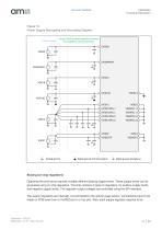
Document Feedback Figure 15: Power Supply Decoupling and Grounding Diagram single 100nF ceramic capacitor as close as possible to each physical pin VDD33 VDDARRAY VDDARRAY Analog ground VSSA VSSACP Digital ground (A/D Converters) Digital ground (Periphery) Biasing (on-chip regulators) Operating the pixel array requires multiple different biasing supply levels. These supply levels can be generated using on-chip regulators. The chip contains 2 types of regulators, for positive supply levels and negative supply levels. The regulator output voltages are controlled using the SPI interface. The supply...
Open the catalog to page 23All AMS catalogs and technical brochures
 TDC-GP21
91 Pages
 NanEye / NanEye Stereo
33 Pages
 CMV20000
48 Pages
 BELICE-850
22 Pages
 CMOSIS company brochure
3 Pages
 CHR70M
2 Pages
 CMV20000
2 Pages
 CMV12000
2 Pages
 CMV4000
2 Pages
 CMV2000
2 Pages


- Resistance temperature sensor
- Proximity switch
- Inductive proximity sensor
- Position transducer
- Thermocouple temperature transducer
- Signal amplifying integrated circuit
- Linear position transmitter
- Analog position transducer
- No-contact position sensor
- Compact temperature probe
- Magnetic position sensor
- Industrial converter
- High-temperature temperature sensor
- Industrial position sensor
- Digital temperature sensor
- Metal position sensor
- Potentiometer position sensor
- Voltage amplifier
- Absolute position sensor