


- Products
- Catalogs
- News & Trends
- Exhibitions
CMV20000

CMV20000
The CMV20000 is a 20 Megapixel global shutter CMOS image sensor with a resolution of 5120 x 3840 pixels, featuring a 6.4μm pixel pitch and supporting a frame rate of 30 fps at full resolution. It includes a programmable gain amplifier, offset regulation, and supports high dynamic range modes with 16 LVDS outputs for data transmission.
The datasheet has been updated to include changes in voltage specifications, timing calculations, and new features like angular response and digital test signals.
The architecture comprises a pixel array, analog front-end electronics, LVDS block, sequencer, SPI, and a temperature sensor, each essential for the sensor's operation and performance.
This section provides detailed instructions on supply settings, biasing, digital input pins, electrical IO specifications, input clock, frame rate calculation, start-up sequence, reset sequence, and SPI programming for configuring and operating the sensor.
Details on LVDS low-level pixel timing, readout timing, pixel remapping, control channels, training data, and test patterns ensure accurate data retrieval from the sensor.
Programming options include exposure modes, high dynamic range mode, windowing, image flipping, subsampling, output mode, and power control, allowing customization of the sensor's performance.
Includes package drawing, assembly drawing, cover glass, color filters, QE and spectral response, and angular response, essential for integrating the sensor into devices.
A comprehensive list of pins and an overview of specifications are provided for reference.
Details on ordering the sensor and recommended handling and soldering procedures ensure proper use and maintenance.
- 5120 x 3840 active pixels
- 30 fps frame rate
- Row windowing and X-Y mirroring
- 16 LVDS outputs at 480MHz
- 12-bit ADC output
- High Dynamic Range mode
- On-chip temperature sensor
- SPI control interface
- Full well charge: 15Ke-
- Sensitivity: 8.3 V/lux.s
- Dark noise: 8e- RMS
- Dynamic range: 66 dB
- Power consumption: 1100mW
The SPI interface is used for writing and reading data to and from sensor registers, with specific timing diagrams provided for both operations.
Frames can be requested via a FRAME_REQ pulse, with internal and external exposure control modes supported.
The control channel provides synchronization and status information, with training data used to align the LVDS receiver with the sensor outputs.
The sensor can generate a test pattern for system testing and calibration.
Offset and gain settings are programmable via sequencer registers, with specific default values provided.
Temperature data is stored in specific registers, with a default value provided.
Includes package drawing, cover glass features, and color filter details, essential for device integration.
Graphs illustrate the typical quantum efficiency and spectral response for the CMV20000.
A graph shows the sensor's relative response to incoming light at various angles.
Key specifications include effective pixels, pixel pitch, imager size, full well charge, conversion gain, temporal noise, dynamic range, shutter type, and more.
Part numbers and package details are provided for ordering the sensor.
Recommendations for soldering and handling to avoid damage and ensure proper maintenance.
Catalog excerpts

Member of the ams Group The technical content of this CMOSIS / AWAIBA document is still valid. Contact information: Headquarters: ams AG Tobelbaderstrasse 30 8141 Premstaetten, Austria Tel: +43 (0) 3136 500 0 e-Mail: [email protected] Please visit our website at www.ams.com
Open the catalog to page 1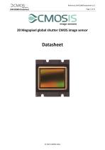
:>CMOS image sensors CMV20000 Datasheet «£CMOSIS image sensors 20 Megapixel global shutter CMOS image sensor
Open the catalog to page 2
:>CMOS image sensors CMV20000 Datasheet Change record Disclaimer CMOSIS reserves the right to change the product, specification and other information contained in this document without notice. Although CMOSIS does its best efforts to provide correct information, this is not warranted. Since the CMV20000 started its design life as a custom imager for traffic applications, the sale of the imager for these applications is excluded.
Open the catalog to page 3
:>CMOS image sensors CMV20000 Datasheet 1 Introduction 1.1 Overview The CMV20000 is a global shutter CMOS image sensor with 5120 by 3840 pixels. The image array consists of 6.4^m x 6.4^m pipelined global shutter pixels which allow exposure during read out, while performing CDS operation. The image sensor has sixteen 12-bit digital LVDS outputs (serial). The image sensor also integrates a programmable gain amplifier and offset regulation. Each channel runs at 480 Mbps maximum which results in 30 fps frame rate at full resolution. Higher frame rates can be achieved in row-windowing mode or row-subsampling...
Open the catalog to page 7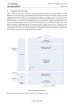
SENSOR ARCHITECTURE Figure 1 shows the image sensor architecture. The internal sequencer generates the necessary signals for image acquisition. The image is stored in the pixel (global shutter) and they are read out sequentially, row-by-row into the analog front-end electronics (AFE) of the columns. On the pixel output, an analog gain of x2.0, x2.4, x2.8 and x3.2 is possible (or 1.6, 1.9, 2.25, 2.55 when column calibration is on). The pixel value then passes to a column ADC cell, in which ADC conversion is performed. The digital signals are then read out over multiple LVDS channels. Each LVDS...
Open the catalog to page 8
2.1 PIXEL ARRAY The CMV20000 sensor has 5120*3840 active pixels with a 6.4um pitch surrounded by two dummy rows and columns. These dummy pixels at the side will ensure that the optical performance, of the active pixels at the edges, is the same as the one in the active array. These dummy pixels cannot be read out and will be set permanent into reset. The pixels are designed to achieve maximum sensitivity with low noise and low PLS specifications. Micro lenses are placed on top of the pixels for improved fill factor and quantum efficiency. 2.2 ANALOG FRONT-END ELECTRONICS (AFE) The analog front...
Open the catalog to page 9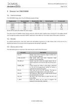
:>CMOS image sensors CMV20000 Datasheet 3 Driving the CMV20000 3.1 Supply settings The CMV20000 image sensor has the following supply settings:
Open the catalog to page 10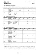
:>CMOS image sensors CMV20000 Datasheet 3.4.1 Digital IO CMOS/TTL DC specifications 3.5 Input clock The high speed LVDS input clock (LVDS_CLK_N/P) defines the output data rate of the CMV20000. The master clock (CLK_IN) must be 12 times slower and this clock but is optional. The maximum data rate of the output is 480Mbps which results in a LVDS_CLK_N/P of 480MHz (and a CLK_IN of 40MHz). The minimum frequencies are 10MHz for CLK_IN and 120MHz for LVDS_CLK_N/P. Any frequency between the minimum and maximum can be applied by the user and will result in a corresponding output data rate.
Open the catalog to page 11
3.6 FRAME RATE CALCULATION The frame rate of the CMV20000 is defined by 2 main factors. 1. 2. Exposure time Read out time For ease of use we will assume that the exposure time is shorter than the read out time. By assuming this, the frame rate is completely defined by the read out time (because the exposure time happens in parallel with the read-out time). The read-out time (and thus the frame rate) is defined by: 1. 2. 3. Output clock speed: max 480Mbps Number of lines read-out Number of outputs used: max 16 LVDS outputs (8 on the top and 8 on the bottom) This means that if any of the parameters...
Open the catalog to page 12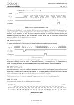
CMV20000 Datasheet Stable time SYS_RES_N FRAME_REQ FIGURE 2: START-UP SEQUENCE FOR 480MBPS @ 12-BIT The CLK_IN and LVDS_CLK_N/P should only start after the rise time of the supplies (VDD33, VDD20, Vddpix and Vres_h go high together). The external reset pin should be released at least 1μs after the supplies have become stable. The first frame can be requested 1μs after the reset pin has been released. An optional SPI upload (to program the sequencer) is possible 1μs after the reset pin has been released. In this case the FRAME_REQ pulse must be postponed until after the SPI upload has been completed....
Open the catalog to page 13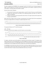
The data is sampled by the CMV20000 on the rising edge of the SPI_CLK. The SPI_CLK has a maximum frequency of 20MHz. The SPI_EN signal has to be high for half a clock period before the first databit is sampled. SPI_EN has to remain high for 1 clock period after the last databit is sampled. One write action contains 16 databits: One control bit: First bit to be sent, indicates whether a read (‘0’) or write (‘1’) will occur on the SPI interface. 7 address bits: These bits form the address of the programming register that needs to be written. The address is sent MSB first. 8 data bits: These...
Open the catalog to page 14
So when sampling on the rising SPI_CLK edge it is advised to have a SPI_CLK of 10MHz maximum. 3.10 REQUESTING A FRAME After starting up the sensor (see section 3.7), a number of frames can be requested by sending a FRAME_REQ pulse. The number of frames can be set by programming the appropriate register (addresses 22 and 23). The default number of frames to be grabbed is 1. In internal-exposure-time mode, the exposure time will start after this FRAME_REQ pulse. In the external-exposuretime mode, the read-out will start after the FRAME_REQ pulse. Both modes are explained into detail in the sections...
Open the catalog to page 15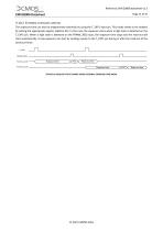
:>CMOS image sensors CMV20000 Datasheet 3.10.2 External exposure control The exposure time can also be programmed externally by using the T_EXP1 input pin. This mode needs to be enabled by setting the appropriate register (address 81). In this case, the exposure starts when a high state is detected on the T_EXP1 pin. When a high state is detected on the FRAME_REQ input, the exposure time stops and the read-out will start automatically. A new exposure can start by sending a pulse to the T_EXP1 pin during or after the read-out of the previous frame. Exposure time Exposure time FIGURE 10: REQUEST...
Open the catalog to page 16All AMS catalogs and technical brochures
 TDC-GP21
91 Pages
 NanEye / NanEye Stereo
33 Pages
 CMV50000
138 Pages
 BELICE-850
22 Pages
 CMOSIS company brochure
3 Pages
 CHR70M
2 Pages
 CMV20000
2 Pages
 CMV12000
2 Pages
 CMV4000
2 Pages
 CMV2000
2 Pages


- Resistance temperature sensor
- Proximity switch
- Inductive proximity sensor
- Position transducer
- Thermocouple temperature transducer
- Signal amplifying integrated circuit
- Linear position transmitter
- Analog position transducer
- No-contact position sensor
- Compact temperature probe
- Magnetic position sensor
- Industrial converter
- Industrial position sensor
- High-temperature temperature sensor
- Digital temperature sensor
- Metal position sensor
- Potentiometer position sensor
- Voltage amplifier
- Absolute position sensor