GC-IP200
1 /31Pages

GC-IP200
1 /31Pages
Catalog excerpts

GC-IP200 Datasheet Version: 2.2 Date: 31/01/2017 AMAC ASIC- und Mikrosensoranwendung Chemnitz GmbH Kopernikusstr. 16 D-09117 Chemnitz Germany
Open the catalog to page 1
Revision History Date First preparation Diverse modifications and additions SPI protocol corrections, supplementation of mechanical and electrical parameters change to new AMAC document layout © Copyright 2017 AMAC ASIC- und Mikrosensoranwendung Chemnitz GmbH Subject to change without prior notice. Our policy is one of continuous improvement, and consequently the equipment may vary slightly from the description and specifications in this publication. The specifications, illustrations and descriptions provided in this documentation are not binding in detail. No part of this publication may be...
Open the catalog to page 2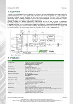
1 Overview The GC-IP200 interpolation circuit is designed for connection to incremental position and angle measuring systems with sine-shaped output signals with a 90° phase shift. It can be operated at a large number of transducer systems working according to the most varied measuring principles. With a maximum interpolation rate of 200 the IC is capable to split the input signal period into up to 200 segments. A counter value can be output via parallel or serial interface, respectively. Different interfaces and flexible configuration types enable the use of the GC-IP200 in single-chip interpolation...
Open the catalog to page 6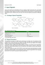
Input Signals 3 Input Signals The two input signals for the interpolation function are analogue voltages (sine/cosine) with a sine-shaped dependency on the measured value (position or angle respectively) with a phase shift of 90° between these two analogue voltages, related to one period of the scale. A third input signal serves as a reference signal for determining the zero or reference point of the scale. All the three input signals are processed as differential signals. 3.1 Analogue Signal Properties Difference Signal Sin = SinP-SinN Angle 0° Vdiff Peak to Peak SinP SinN 90° Phase Shift Vdiff...
Open the catalog to page 7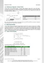
Input Signals 3.3 Reference Signals / Index Point A third output of the measuring system - typically called reference, index point or zero point signal considered to be activated, if the difference of the signals at the REFP and REFN pins becomes greater than the positive hysteresis voltage VRPH and is considered to be deactivated if this voltage becomes smaller than the negative hysteresis voltage VRPL. REFN REFP respectively: VRPH VRPL VRPL (typical) Hysteresis (typical) VRPH (typical) Figure 3: Reference Signals If a sensor without reference signals is used, defined levels on pins REFP and...
Open the catalog to page 8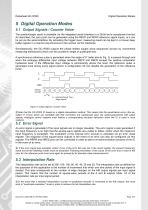
Digital Operation Modes 5 Digital Operation Modes 5.1 Output Signals / Counter Value The position/angle result is available via the integrated serial interface in a 28-bit two's-complement format. As described, the zero point can be generated using the REFP and REFN reference signal inputs, or it can be set via the serial interface. By activating the trigger input, measuring result can be kept in a 2-level deep buffer register in a manner asynchronous to the access via the interfaces. Simultaneously, the GC-IP200 outputs the phase shifted square wave sequences (known by incremental measuring...
Open the catalog to page 9
Digital Operation Modes 5.4 Interval Time / Maximum Input Frequency The interval time (IT) and the minimum edge distance tpp at the output signals, respectively, can be set in binary steps at values between 1/fosz and 128/fosz. In counter mode (the SPEED Bit in the CFG0 Register being set), the maximum input frequency totals fmax=fosc /96. In all the other modes, the maximum input frequency is limited by the minimum pulse distance at the output, where: fmax 0.9*fOSZ /(IRIT) < fosz/96 fosc: Clock frequency at Pin XA IR: Activated Interpolation Rate IT: Activated Interval Time The limit values...
Open the catalog to page 10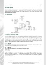
6 Interfaces The measurement results can be read out over the integrated serial interface (SPI). It is also possible to make a more detailed configuration of the GC-IP200 IC over this interface than over hardware. For high speed applications the additional 16-bit wide parallel port allow to read out the measurement results continuously with up to 32MBit/s. 6.1 Structure WR-Register Bank Cycle Counter C-CNT Figure 6: interface structure 6.2 Serial Interface (SPI) The serial interface contains a 16-bit shift register for read accesses and write accesses each. An additional 16-bit hold register...
Open the catalog to page 11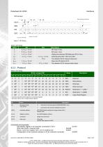
Start command processing SCLK tVDI tSETDI tRDY Figure 7: SPI timing Table 4: SPI timing Name SPI clock, H time SPI clock, L time Waiting time between SEN falling and SCLK rising 4 x TOSZ + 15 ns Switching delay RDY / SDO from SEN Time between SCLK rising and data read Setup time SDI before SCLK 5 TOSZ + 15 ns Time between SCLK rising and data output 6.2.2 Protocol Table 5: SPI timing Bit No. at signal SDI 15 Write Address Write Data Write Command Output Read-Register command load the internal data into a 32-bit hold register 2) bit must be set to zero in single-channel systems Bit Broadcast mode...
Open the catalog to page 12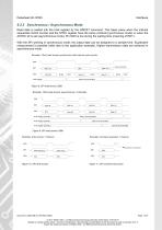
6.2.3 Synchronous / Asynchronous Mode Read data is loaded into the hold register by the RD0/ST command. This takes place when the internal sequential control counter and the SYNC register have the same contents (synchronous mode) or when the ASYNC bit is set (asynchronous mode). Pin SDO is low during the waiting time (meaning of RDY) . With the SPI working in synchronous mode, the output data can be assigned to a sample time. Equidistant measurement is possible (refer also to the application example). Higher transmission rates are achieved in asynchronous mode. Example: 32-bit read access synchronous...
Open the catalog to page 13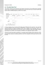
6.3 Parallel Data Port This interface outputs the last activated SPI read register synchronized to the GC-IP200 internal sequential control counter. The appearing data are separated into two 16-bit words. After reset, the data of the SPI read register address 0x00(MVAL)appears on DATA(15:0) by default. Sequential Control Counter OUTHIGH STRB XA Signal TDelay TDelay < 15ns Figure 12: timing Parallel Data Port To reduce switching noise on the data port the Data outputs DATA(15:8) will be switched 1 clock cycle after the outputs DATA(7:0). That's why the value at DATA(15:8) is undefined in the clock...
Open the catalog to page 14All AMAC ASIC - und Mikrosensoranwendung Chemnitz GmbH catalogs and technical brochures
 AIP40
AIP4019 Pages
 GC-IP201 / GC-IP201(B)
59 Pages
 GC-IP1000B
33 Pages
 GC-NIP
65 Pages
 AM-IP4k
54 Pages
 AM-CVC2D
36 Pages
 Level shifter GC-LS
13 Pages
 GC-IP2000
51 Pages
- Acceleration sensor
- Single-axis accelerometer
- Programmable amplifier
- Photodiode microchip
- 2-channel amplifier
- Vibrating accelerometer
- Digital output accelerometer
- Digital microchip
- Power integrated circuit
- Programmable integrated circuit
- Interpolator
- Measuring system interpolator
- Interpolator with ABZ interface
- Interpolator with BiSS interface