AM-CVC2D
1 /36Pages
AM-CVC2D
1 /36Pages
Catalog excerpts

Datasheet Version: 0.1 Datum: 15/04/2021 AMAC ASIC- und Mikrosensoranwendung Chemnitz GmbH Kopernikusstr. 16 D-09117 Chemnitz Germany
Open the catalog to page 1
Revision history Date First version © Copyright 2021 AMAC ASIC- und Mikrosensoranwendung Chemnitz GmbH Subject to change without prior notice. Our policy is one of continuous improvement, and consequently the equipment may vary slightly from the description and specifications in this publication. The specifications, illustrations and descriptions provided in this documentation are not binding in detail. No part of this publication may be reproduced in any form, or by any means, without the prior written permission of AMAC ASIC- und Mikrosensoranwendung Chemnitz GmbH. All rights according to the...
Open the catalog to page 2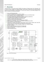
The AM-CVC2D is a two-channel charge amplifier with analogue and digital outputs, fully configurable. The IC serves for sensor excitation and charge evaluation. The IC uses as charge input two external capacitive sensors and can be controlled via a serial protocol. The AM-CVC2D consists of a mixed-signal integrated circuit, which is composed of the following components: Sensor controlling/optimization. 10 bit DAC for adjustment of the excitation voltages. Driver for generation of the recharging voltages for continuous and self-test modes. Internal reference voltage via adjustable band gap Two...
Open the catalog to page 6
Table 1: General technical specifications Parameter Characteristic value Operating voltage: Current consumption: Operating temperature range: Internal RC oscillator set to a nominal frequency of 40 MHz Configurable carrier frequency Reference voltage: (VREF) Can be set in 16 steps each of 8 mV (4 bit), nominal 1.2 V Resetting of all registers Loading of configuration from the integrated EEPROM Start time, including EEPROM read-out at 150 KHz: nominal 10.5 ms Driver for sensor excitation: Generation of the recharging voltages XEP/XEN and YEP/YEN Voltages are configured symmetrically to VREF =...
Open the catalog to page 7
Table 2: Pin description Pin Nr. CLDCCJ28 Single-Chip Analogue voltage supply X-channel, XE1 excitation voltage output X-channel, charge amplifier input X-channel, XE2 excitation voltage output Buffered reference voltage Buffered reference voltage Y-channel, YE2 excitation voltage output Y-channel, input charge amplifier Y-channel, YE1 excitation voltage output Buffered reference voltage XY-channel, test pin sensor output voltage I2C slave address select I2C slave address select Reset and Stand-By, L-active (I=ext. Reset; O=Status internal POR) SPI (Slave mode), Chip-Select, L-active I2C: Clock...
Open the catalog to page 8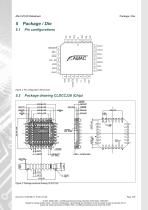
Package drawing CLDCCJ28 (Chip) Figure 3: Package technical drawing CLDCCJ28 Document: 51600-DB-0-1-E-AM_CVC2D © 2021 AMAC ASIC- und Mikrosensoranwendung Chemnitz GmbH Date: 15/04/2021 Subject to change without notice · Any kind of duplication, reprocessing and translation of this document as well as excerpts from it require the written permission of AMAC ASIC- und Mikrosensoranwendung Chemnitz GmbH.
Open the catalog to page 9
Functional description Functional description Reference voltage Source of the internal reference voltages REFM, REFH, REFL Table 3: Parameter reference voltage Parameter Mean reference voltage REFM* (Charge amplifier) High reference voltage REFH (ADC) Low reference voltage REFL (ADC) Increment for VREFB adjustment (4Bit) Offset voltage OPV buffered VREFB Accuracy as function of temperature, at AVDD = 3.3V *Adjustment is performed by the manufacturer D/A converter with a 10 bit resolution for the supply of the programmable voltages VXP, VXN, VYP, and VYN are the amplitude settings for the sensor...
Open the catalog to page 10
Functional description Table 6: Detuning examples for VXPEP Parameter Resulting detuning Charge amplifiers (X_CHAMP, Y_CHAMP) Charge amplifiers with programmable offset and integration capacitances The integration capacitance values can be set at the sensor control registers XCINT and YCINT for each channel. Also at XCOFF and YCOFF registers for the offset capacitance values. For the integration capacitances the range value goes from 0 to 12.7 pF and is incremented in 0.1 pF steps. And for the offset capacitances the range value goes from 0 to 3.175 pF and is incremented in 0.025 pF steps. Table...
Open the catalog to page 11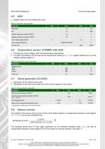
Functional description Single Ended and Fully Differential mode Table 8: Parameter output amplifier Parameter Positive reference voltage (VREFP) Negative reference voltage (VREFN) Input voltage single Ended Input voltage differential Sample rate Temperature sensor (VTEMP) with ADC Providing an output voltage, with lineal temperature dependency. The ADC temperature can be read as the temperature reading at ADCTEMP register address 34 or as the voltage reading register 41. Table 9: Temperature sensor parameters Parameters Rising rate Clock generator (CLOCK) Generation of the internal clock pulse...
Open the catalog to page 12
Functional description Table 11: Sensor clock division per sampling mode Sampling mode Dual single-ended sampling (OPM1 = '1') The settings for STPCLKVAL and OPM1 should be selected so that the maximum sensor frequency of 500 KHz is not exceeded. Table 12: Maximum adjustable sensor frequency as per mode Resulting Sensor clock1 STPCLKVAL (Decimal) Single-ended sampling (OPM1 = '0'), one channel Dual single-ended sampling (OPM1 = '1'), one channel Single-ended sampling (OPM1 = '0'), two channel Dual single-ended Sampling (OPM1 = '1'), two channel Furthermore the piezo mode can be enabled via the...
Open the catalog to page 13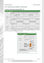
Functional description 6.8.1 Timing sensor excitation / normal mode 1-channel, single-ended sampling (OPM1 = '0') Signal CLOCK Figure 4: Timing sensor excitation (1-channel, single-ended sampling) Sensor excitation power on cycle Signal CLOCK REFN1 %---------#___@====^ VREF REFP2 ^=========!___$----% Sensor DISCHARGE: Sensor DISCHARGE: EP and EN short-circuited EP and EN short-circuited Figure 5: Sensor excitation power on cycle Document: 51600-DB-0-1-E-AM_CVC2D © 2021 AMAC ASIC- und Mikrosensoranwendung Chemnitz GmbH Date: 15/04/2021 Subject to change without notice · Any kind of duplication,...
Open the catalog to page 14
Functional description 1-channel, dual single-ended sampling (OPM1 = '1') Signal CLOCK ^==================\-----------------------/==========^ %------------------/=======================\----------% Figure 6: Timing sensor excitation (1-channel, dual single-ended sampling) 2-channel, single-ended sampling (OPM1 = '0') Signal CLOCK Figure 7: Timing sensor excitation (2-channel, single-ended sampling) Document: 51600-DB-0-1-E-AM_CVC2D © 2021 AMAC ASIC- und Mikrosensoranwendung Chemnitz GmbH Date: 15/04/2021 Subject to change without notice · Any kind of duplication, reprocessing and translation...
Open the catalog to page 15All AMAC ASIC - und Mikrosensoranwendung Chemnitz GmbH catalogs and technical brochures
 AIP40
AIP4019 Pages
 GC-IP200
31 Pages
 GC-IP201 / GC-IP201(B)
59 Pages
 GC-IP1000B
33 Pages
 GC-NIP
65 Pages
 AM-IP4k
54 Pages
 Level shifter GC-LS
13 Pages
 GC-IP2000
51 Pages
- Acceleration sensor
- Single-axis accelerometer
- Programmable amplifier
- Photodiode microchip
- 2-channel amplifier
- Vibrating accelerometer
- Digital output accelerometer
- Digital microchip
- Power integrated circuit
- Programmable integrated circuit
- Interpolator
- Measuring system interpolator
- Interpolator with ABZ interface
- Interpolator with BiSS interface