- Catalogs
- ALLEGRO MICROSYSTEMS
- Low-Cost Single-Inductor Triple-Output TFT LCD Supply
Low-Cost Single-Inductor Triple-Output TFT LCD Supply
1 /2Pages

Low-Cost Single-Inductor Triple-Output TFT LCD Supply
1 /2Pages
Catalog excerpts
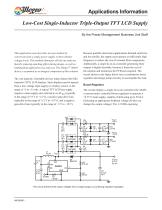
Applications Information Low-Cost Single-Inductor Triple-Output TFT LCD Supply By the Power Management Business Unit Staff This application note describes an easy method of conversion from a single power supply to three distinct voltage levels. This method eliminates all but one inductor, thereby reducing matching effort during design, as well as limiting final application size and cost. The Allegro™ A8483 device is examined as an integral component of this solution. The vast majority of portable devices today feature thin-film transistor (TFT) LCD displays. Such displays need to operate from a low-voltage input supply or a battery source, in the range of +3 to +5 volts. A typical TFT LCD bias supply requires a main supply, also referred to as AVDD (typically in the range of +8 V to +12 V), a positive gate-drive bias (typically in the range of +12 V to +18 V), and a negative gate-drive bias (typically in the range of –5 V to –10 V). Because portable electronics applications demand small size and low profile, the supply must operate at sufficiently high frequency to reduce the size of external filter components. Additionally, a single dc-to-dc controller generating three outputs is highly desirable, because it limits the cost of the solution and minimizes the PCB area required. The circuit shown in the figure below uses a combination boost regulator and charge pump circuitry to accomplish this task. Boost Regulator The circuit employs a single dc-to-dc controller (the A8483, a current-mode–controlled boost regulator) to generate a +8.75 V main supply, capable of delivering up to 50 mA. (Selecting an appropriate feedback voltage divider can change the output voltage.) The 1.2 MHz operating This circuit delivers three output voltages from a single supply, by combining regulator topologies.
Open the catalog to page 1
frequency reduces the inductor size and allows operation with tiny ceramic capacitors. Internal compensation simplifies circuit design and reduces external component count. The low-profile (0.75 mm nominal height) MLP/TDFN package allows the boost regulator to be mounted on either side of the PCB to optimize footprint and minimize height. Positive and Negative Charge Pumps When the internal switch of the A8483 is on, the SW node is near 0 V, with low impedance to circuit ground. When the internal switch of the A8483 switches off in order to provide boost action, the SW node goes up to approximately...
Open the catalog to page 2All ALLEGRO MICROSYSTEMS catalogs and technical brochures
 A1340
A134042 Pages
 A1324
A132412 Pages
 A1318
A131812 Pages
 A1308
A130812 Pages
 A1304
A130410 Pages
 A1367
A136727 Pages
 A1366
A136622 Pages
 A1365
A136532 Pages
 ACS770
29 Pages
 ACS758
22 Pages
 ACS761
14 Pages
 A1301 and A1302
10 Pages
 ACS709
17 Pages
 ACS716
22 Pages
 ACS715
14 Pages
 ACS714
18 Pages
 ACS712
15 Pages
 ACS713
14 Pages
 ACS756
11 Pages
 ACS710
23 Pages
 ACS711
16 Pages
 A1360, A1361, and A1362
26 Pages
 ACS759
19 Pages
 Advances in WLED/RGB LED Drivers
13 Pages


Archived catalogs
 A6261: Protected LED Array Driver
14 Pages
 Current Sensors
9 Pages


- Lumibird single-pole switch
- Lumibird proximity sensor
- Lumibird technology switch
- Position transducer
- Lumibird multipole switch
- Motor controller
- Linear position transmitter
- Analog position transducer
- No-contact position sensor
- Stepper motor controller
- Magnetic position sensor
- Bipolar switch
- Industrial position sensor
- Magnetic proximity sensor
- Lumibird speed controller
- Magnetic speed sensor
- Angular position sensor
- Rotational speed sensor
- Motor driver
- Precision position sensor