- Catalogs
- ALLEGRO MICROSYSTEMS
- A1444 and A1445 Low-Voltage Full-Bridge Brushless DC Motor Driver with Hall Commutation, Externally Controlled Speed Regulation, Soft Switching, and Reverse Battery, Short Circuit, and Thermal Shutdown Protection
A1444 and A1445 Low-Voltage Full-Bridge Brushless DC Motor Driver with Hall Commutation, Externally Controlled Speed Regulation, Soft Switching, and Reverse Battery, Short Circuit, and Thermal Shutdown Protection

A1444 and A1445 Low-Voltage Full-Bridge Brushless DC Motor Driver with Hall Commutation, Externally Controlled Speed Regulation, Soft Switching, and Reverse Battery, Short Circuit, and Thermal Shutdown Protection
Catalog excerpts
VDD Reverse Battery Output Full Bridge Q1Q3Q2Q4 SLEEP Power and SleepMode Control Active BrakingControl Drive LogicandSoft SwitchingControl GND VOUT1 Stall Detection 0.1 F VOUT2 AmHallElementp M Thermal ShutdownProtection PDC > ESD PWMControl >
Open the catalog to page 1
CharacteristicsSymbolTest ConditionsMin.Typ. > 1 Max.Unit Supply Voltage V > DD T > J < T > J (max) 2.0 4.2 V Extended Supply Voltage > 2 V > DDE T > J < T > J (max) 1.8 ֖4.2 V Supply Current I > IN >V > INHI , T > A = 25C, no load Ж4 6 mA V > DD(ON) V > IN < V > INLO , T > A = 25C Ж10 A Total Output On-Resistance I > OUT = 50 mA, V > DD = 2 V, T > A = 25ְC 3.9 ֖I > 3 R > DS(on) OUT = 50 mA, V > DD = 3 V, T > A = 25C Ж2.6 I > OUT = 50 mA, V > DD = 4 V, T > A = 25ְC 2.2 ֖ Reverse Battery CurrentI V > RDD = 4.2 V, current flowing out of VDD pin, T > RDD A = 25ְC ֖10 mA ֯S ϯL ϯE ϯE ϯP Input Threshold...
Open the catalog to page 3
CharacteristicsSymbolTest ConditionsMin.Typ. > 1 Max.Unit > OP 2 V V > DD 4 V35 75 G B Magnetic SwitchpointsB > RP 2 V V > DD 4 V֖75 35 ֖G B > HYS 2 V V > DD 4 V70 ֖G Output Polarity VOUT1B < B > RP LOW֖VB > B > OP HIGH֖VVOUT2B < B > RP HIGH ֖VB > B > OP LOW֖V > 1 Typical data are for initial design estimations only, and assume optimum manufacturing and application conditions, such as T > A = 25C. Performance may vary for individual units, within the specified maximum and minimum limits. > 2 Device operates with lower supply voltages, down to 1.8 V, with slight variation in specification of magnetic...
Open the catalog to page 4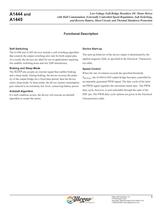
Device Start-up The start-up behavior of the device output is determined by the applied magnetic field, as specified in the Electrical Characteris- tics table. Speed Control > When the rate of rotation exceeds the specified threshold, S > Antistall Algorithm Soft Switching Braking and Sleep Mode If a stall condition occurs, the device will execute an antistall algorithm to restart the motor. The A1444 and A1445 devices include a soft switching algorithm that controls the output switching slew rate for both output pins. As a result, the devices are ideal for use in applications requiring low audible...
Open the catalog to page 5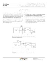
Allegro MicroSystems, Inc.115 Northeast CutoffWorcester, Massachusetts 01615-0036 U.S.A.1.508.853.5000; www.allegromicro.com >
Open the catalog to page 6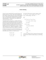
The device must be operated below the maximum junction tem-perature of the device, T > J (max). Under certain combinations of peak conditions, reliable operation may require derating supplied power or improving the heat dissipation properties of the appli- cation. This section presents a procedure for correlating factors affecting operating T > A = 25C, V > DD = 3 V, I > DD = 85 mA, V > LOAD = 2.43 V, I > LOAD = 83 mA, and R > JA = 250 аC/W, then: P > J . (Thermal data is also available on the Allegro MicroSystems website.)The package thermal resistance, R > D = V > DD I > DD ז V > LOAD I > LOAD...
Open the catalog to page 7All ALLEGRO MICROSYSTEMS catalogs and technical brochures
 A1340
A134042 Pages
 A1324
A132412 Pages
 A1318
A131812 Pages
 A1308
A130812 Pages
 A1304
A130410 Pages
 A1367
A136727 Pages
 A1366
A136622 Pages
 A1365
A136532 Pages
 ACS770
29 Pages
 ACS758
22 Pages
 ACS761
14 Pages
 A1301 and A1302
10 Pages
 ACS709
17 Pages
 ACS716
22 Pages
 ACS715
14 Pages
 ACS714
18 Pages
 ACS712
15 Pages
 ACS713
14 Pages
 ACS756
11 Pages
 ACS710
23 Pages
 ACS711
16 Pages
 A1360, A1361, and A1362
26 Pages
 ACS759
19 Pages
 Advances in WLED/RGB LED Drivers
13 Pages


Archived catalogs
 A6261: Protected LED Array Driver
14 Pages
 Current Sensors
9 Pages


- Lumibird single-pole switch
- Lumibird proximity sensor
- Lumibird technology switch
- Position transducer
- Lumibird multipole switch
- Motor controller
- Linear position transmitter
- Analog position transducer
- No-contact position sensor
- Stepper motor controller
- Magnetic position sensor
- Bipolar switch
- Industrial position sensor
- Magnetic proximity sensor
- Lumibird speed controller
- Magnetic speed sensor
- Angular position sensor
- Rotational speed sensor
- Motor driver
- Precision position sensor