- Catalogs
- ALLEGRO MICROSYSTEMS
- A1441 Low-Voltage Full-Bridge Brushless DC Motor Driver with Hall Element Commutation
A1441 Low-Voltage Full-Bridge Brushless DC Motor Driver with Hall Element Commutation

A1441 Low-Voltage Full-Bridge Brushless DC Motor Driver with Hall Element Commutation
Catalog excerpts

Date of status change: November 1, 2008These parts are in production but have been determined to be NOT FOR NEW DESIGN. This classification indicates that sale of this device is currently restricted to existing customer applications. The device should not be purchased for new design applications because obsolescence in the near future is probable. Samples are no longer available. NOTE: For detailed information on purchasing options, contact your local Allegro field applications engineer or sales representative. > Allegro MicroSystems, Inc. reserves the right to make, from time to time, revisions to the anticipated product life cycle plan for a product to accommodate changes in production capabilities, alternative product availabilities, or market demand. The information included herein is believed to be accurate and reliable. However, Allegro MicroSystems, Inc. assumes no respon- sibility for its use; nor for any infringements of patents or other rights of third parties which may result from its use. size="-1">
Open the catalog to page 1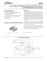
Features and Benefits Description > Single-chip solution for high reliability Chopper stabilization technique for precise signal response over operating range 2.0 to 4.0 V operation Sleep mode pin allowing external logic signal enable/disable to reduce average power consumption Restart feature Small package size The A1441 is a full-bridge motor driver designed to drive low-voltage bipolar brushless dc motors. Commutation of the motor is achieved by use of a single Hall element sensor to detect the position of an alternating-pole ring magnet. A high density merged Bipolar-CMOS semiconductor process...
Open the catalog to page 2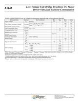
DEVICE CHARACTERISTICS over the voltage and temperature operating range, unless otherwise specifiedCharacteristicsSymbolTest ConditionsMin.Typ.Max.Units Supply VoltageV > DD Running2.04.0VTotal Output Saturation Voltage > 1 V I > LOAD = 100 mA, V > DD = 3.6 V֖500mVI > OUT(Sat) LOAD = 70 mA, V > DD = 2.2 V֖400mVSleep Mode Supply CurrentI > DD(Sleep) ֖10ALoad Current Rise Time > 2 t > r(ILOAD) V > DD = 3.6 V֖10sChopping Settling Time > 3 t > s(CHOP) ֖30s֯S ϯL ϯE ϯE ϯP Input ThresholdV > INLO ϖ0.5VV > INHI V > DD ֖0.7֖VSϯ Lϯ Eϯ Eϯ Pϯ Input CurrentI > IN ֖1ACrossover Dead Time > 4 t > DT VOUT switching2֖sRestart...
Open the catalog to page 4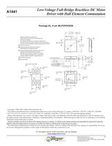
2.15 1.85.085.073 A > D 1.00.0394 B > DE 1.00.0394 ATerminal #1 mark area 2.15 1.85.085.073 BExposed thermal pad (reference only, terminal #1 identifier appearance at supplier discretion) Hall element (not to scale) Preliminary dimensions, for reference only(JEDEC ultra-thin MO-229UCCD, except contact layout) Dimensions in millimeters U.S. Customary dimensions (in.) in brackets, for reference only Dimensions exclusive of mold flash, gate burrs, and dambar protrusions Exact case and lead configuration at supplier discretion within limits shown A C DActive area depth 0.08 [.003]6X C SEATINGPLANE...
Open the catalog to page 5All ALLEGRO MICROSYSTEMS catalogs and technical brochures
 A1340
A134042 Pages
 A1324
A132412 Pages
 A1318
A131812 Pages
 A1308
A130812 Pages
 A1304
A130410 Pages
 A1367
A136727 Pages
 A1366
A136622 Pages
 A1365
A136532 Pages
 ACS770
29 Pages
 ACS758
22 Pages
 ACS761
14 Pages
 A1301 and A1302
10 Pages
 ACS709
17 Pages
 ACS716
22 Pages
 ACS715
14 Pages
 ACS714
18 Pages
 ACS712
15 Pages
 ACS713
14 Pages
 ACS756
11 Pages
 ACS710
23 Pages
 ACS711
16 Pages
 A1360, A1361, and A1362
26 Pages
 ACS759
19 Pages
 Advances in WLED/RGB LED Drivers
13 Pages


Archived catalogs
 A6261: Protected LED Array Driver
14 Pages
 Current Sensors
9 Pages


- Lumibird single-pole switch
- Lumibird proximity sensor
- Lumibird technology switch
- Position transducer
- Lumibird multipole switch
- Motor controller
- Linear position transmitter
- Analog position transducer
- No-contact position sensor
- Stepper motor controller
- Magnetic position sensor
- Bipolar switch
- Industrial position sensor
- Magnetic proximity sensor
- Lumibird speed controller
- Magnetic speed sensor
- Angular position sensor
- Rotational speed sensor
- Precision position sensor