
Catalog excerpts
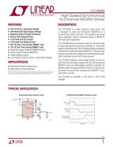
LTC4449 1 4449fa n 4V to 6.5V VCC Operating Voltage n 38V Maximum Input Supply Voltage n Adaptive Shoot-Through Protection n Rail-to-Rail Output Drivers n 3.2A Peak Pull-Up Current n 4.5A Peak Pull-Down Current n 8ns TG Rise Time Driving 3000pF Load n 7ns TG Fall Time Driving 3000pF Load n Separate Supply to Match PWM Controller n Drives Dual N-Channel MOSFETs n Undervoltage Lockout n Low Profi le (0.75mm) 2mm × 3mm DFN Package TYPICAL APPLICATION FEATURES APPLICATIONS DESCRIPTION High Speed Synchronous N-Channel MOSFET Driver The LTC®4449 is a high frequency gate driver that is designed to drive two N-Channel MOSFETs in a synchronous DC/DC converter. The powerful rail-to-rail driver capability reduces switching losses in MOSFETs with high gate capacitance. The LTC4449 features a separate supply for the input logic to match the signal swing of the controller IC. If the input signal is not being driven, the LTC4449 activates a shutdown mode that turns off both external MOSFETs. The input logic signal is internally level-shifted to the bootstrapped supply, which functions at up to 42V above ground. The LTC4449 contains undervoltage lockout circuits on both the driver and logic supplies that turn off the external MOSFETs when an undervoltage condition is present. An adaptive shoot-through protection feature is also built-in to prevent the power loss resulting from MOSFET crossconduction current. The LTC4449 is available in the 2mm × 3mm DFN package. Synchronous Buck Converter Driver n Distributed Power Architectures n High Density Power Modules LTC4449 Driving 3000pF Capacitive Loads TG BOOST VIN TO 38V GND TS VLOGIC VCC LTC4449 PWM BG VCC 4V TO 6.5V IN VOUT 4449 TA01a TOP GATE (TG - TS) 5V/DIV INPUT (IN) 5V/DIV 4449 TA01b BOTTOM GATE (BG) 5V/DIV 10ns/DIV L, LT, LTC, LTM, Linear Technology and the Linear logo are registered trademarks of Linear Technology Corporation. All other trademarks are the property of their respective owners.
Open the catalog to page 1
LTC4449 3 4449fa The l denotes the specifi cations which apply over the full operating junction temperature range, otherwise specifi cations are at TA = 25°C. VCC = VLOGIC = VBOOST = 5V, VTS = GND = 0V, unless otherwise noted. (Note 2) Note 1: Stresses beyond those listed under Absolute Maximum Ratings may cause permanent damage to the device. Exposure to any Absolute Maximum Rating condition for extended periods may affect device reliability and lifetime. Note 2: The LTC4449 is tested under pulsed load conditions such that TJ TA. The LTC4449E is guaranteed to meet specifi cations from 0°C...
Open the catalog to page 3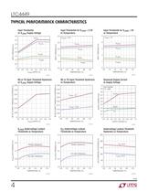
LTC4449 4 4449fa TYPICAL PERFORMANCE CHARACTERISTICS Input Thresholds vs VLOGIC Supply Voltage Input Thresholds for VLOGIC = 3.3V vs Temperature BG or TG Input Threshold Hysteresis vs VLOGIC Supply Voltage VLOGIC Undervoltage Lockout Thresholds vs Temperature Undervoltage Lockout Threshold Hysteresis vs Temperature Input Thresholds for VLOGIC 5V vs Temperature Quiescent Supply Current vs Supply Voltage VCC Undervoltage Lockout Thresholds vs Temperature BG or TG Input Threshold Hysteresis vs Temperature VLOGIC SUPPLY (V) 3.0 3.5 0 INPUT THRESHOLD (V) 1.0 4.0 4.0 5.0 5.5 4449 G01 0.5 2.0 2.5...
Open the catalog to page 4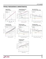
LTC4449 5 4449fa TYPICAL PERFORMANCE CHARACTERISTICS Supply Current vs Input Frequency Propagation Delay vs VLOGIC Supply Voltage Propagation Delay vs VCC (Boost) Supply Voltage Rise and Fall Time vs VCC (Boost) Supply Voltage Switching Supply Current vs Load Capacitance Rise and Fall Time vs Load Capacitance Propagation Delay vs Temperature FREQUENCY (Hz) 0 5 6 800k 4449 G12 4 3 200k 400k 600k 1M 2 1 0 SUPPLY CURRENT (mA) NO LOAD VLOGIC = VCC = 5V TS = GND IVCC IVLOGIC LOAD CAPACITANCE (nF) 0.1 SUPPLY CURRENT (mA) 1 10 100 4449 G13 3 10 30 VLOGIC = VCC = 5V TS = GND ICC fIN = 500kHz ICC...
Open the catalog to page 5
LTC4449 6 4449fa BLOCK DIAGRAM PIN FUNCTIONS TG (Pin 1): High Side Gate Driver Output (Top Gate). This pin swings between TS and BOOST. TS (Pin 2): High Side MOSFET Source Connection (Top Source). BG (Pin 3): Low Side Gate Driver Output (Bottom Gate). This pin swings between VCC and GND. GND (Pin 4, Exposed Pad Pin 9): Chip Ground. The exposed pad must be soldered to PCB ground for optimal electrical and thermal performance. IN (Pin 5): Input Signal. Input referenced to an internal supply baised off of VLOGIC (Pin 6) and GND. If this pin is fl oating, an internal resistive divider triggers...
Open the catalog to page 6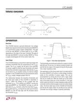
LTC4449 7 4449fa OPERATION TIMING DIAGRAM Figure 1. Three-State Input Operation VIL(BG) VIL(TG) VIL(BG) 90% IN TG BG 90% 10% tr(TG) tpLH(TG) 10% tr(BG) 4449 TD tf(BG) tf(TG) tpLH(BG) tpHL(BG) tpHL(TG) Overview The LTC4449 receives a ground-referenced, low voltage digital input signal to drive two N-channel power MOSFETs in a synchronous power supply confi guration. The gate of the low side MOSFET is driven either to VCC or GND, depending on the state of the input. Similarly, the gate of the high side MOSFET is driven to either BOOST or TS by a supply bootstrapped off of the switch node...
Open the catalog to page 7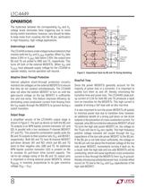
LTC4449 8 4449fa OPERATION Rise/Fall Time Since the power MOSFETs generally account for the majority of power loss in a converter, it is important to quickly turn them on and off, thereby minimizing the transition time and power loss. The LTC4449’s peak pullup current of 3.2A for both BG and TG produces a rapid turn-on transition for the MOSFETs. This high current is capable of driving a 3nF load with an 8ns rise time. It is also important to turn the power MOSFETs off quickly to minimize power loss due to transition time; however, an additional benefi t of a strong pull-down on the driver...
Open the catalog to page 8
LTC4449 9 4449fa APPLICATIONS INFORMATION OPERATION The LTC4449’s powerful parallel combination of the N-channel MOSFET (N2) and NPN (Q3) on the BG pull-down generates a phenomenal 4ns fall time on BG while driving a 3nF load. Similarly, the 0.8Ù pull-down Power Dissipation To ensure proper operation and long-term reliability, the LTC4449 must not operate beyond its maximum temperature rating. Package junction temperature can be calculated by: TJ = TA + (PD)(èJA) where: TJ = junction temperature TA = ambient temperature PD = power dissipation èJA = junction-to-ambient thermal resistance...
Open the catalog to page 9All ADI catalogs and technical brochures
-
 LTC2068
30 Pages
-
 LTC6373
34 Pages
-
 ADL9006
16 Pages
-
 ADL8104
23 Pages
-
 AD4115
52 Pages
-
 ADUM7702
22 Pages
-
 AD7383
33 Pages
-
 AD7384
33 Pages
-
 AD4114
49 Pages
-
 ADUM7704
22 Pages
-
 AD7134
86 Pages
-
 LTspice IV
53 Pages
-
 New Products Catalog
43 Pages
-
 RF/IF Amplifiers
9 Pages
-
 SAR ADC Drivers
2 Pages
-
 SmartMesh Brochure
8 Pages
-
 INDUSTRIAL SIGNAL CHAIN
24 Pages
-
 AUTOMOTIVE ELECTRONIC SOLUTIONS
48 Pages
-
 Battery Management Solutions
32 Pages
-
 DC/DC uModule Power Products
32 Pages
-
 Wireless & RF Solution
36 Pages
-
 LT6656 - 1
18 Pages


Archived catalogs
-
 New Products Catalog
39 Pages
-
 Power Management for LEDs
24 Pages
-
 High Speed ADC Products Brochure
14 Pages


