
Catalog excerpts
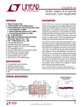
1Msps Throughput Rate 16-Bit Resolution with No Missing Codes 8-Channel Multiplexer with Selectable Input Range n Fully Differential (±4.096V) n Pseudo-Differential Unipolar (0V to 4.096V) n Pseudo-Differential Bipolar (±2.048V) INL: ±1LSB (Maximum) SNR: 96dB (Fully Differential)/93.4dB (PseudoDifferential) (Typical) at fIN = 1kHz n THD: –110dB (Typical) at f = 1kHz IN n Programmable Sequencer n Selectable Digital Gain Compression n Single 5V Supply with 1.8V to 5V I/O Voltages n SPI-Compatible Serial I/O n Onboard 2.048V Reference and Reference Buffer n No Pipeline Delay, No Cycle Latency n Power Dissipation 40mW (Typical) n Guaranteed Operation to 125°C n 32-Lead 5mm × 5mm QFN Package The LTC®2373-16 is a low noise, high speed, 8-channel 16-bit successive approximation register (SAR) ADC. Operating from a single 5V supply, the LTC2373-16 has a highly configurable, low crosstalk 8-channel input multiplexer, supporting fully differential, pseudo-differential unipolar and pseudo-differential bipolar analog input ranges. The LTC2373-16 achieves ±1LSB INL (maximum) in all input ranges, no missing codes at 16-bits and 96dB (fully differential)/ 93.4dB (pseudo-differential) SNR (typical). Programmable Logic Controllers Industrial Process Control High Speed Data Acquisition Portable or Compact Instrumentation ATE The LTC2373-16 has an onboard low drift (20ppm/°C max) 2.048V temperature-compensated reference and a singleshot capable reference buffer. The LTC2373-16 also has a high speed SPI-compatible serial interface that supports 1.8V, 2.5V, 3.3V and 5V logic through which a sequencer with a depth of 16 may be programmed. An internal oscillator sets the conversion time, easing external timing considerations. The LTC2373-16 dissipates only 40mW and automatically naps between conversions, leading to reduced power dissipation that scales with the sampling rate. A sleep mode is also provided to reduce the power consumption of the LTC2373-16 to 300μW for further power savings during inactive periods. L, LT, LTC, LTM, Linear Technology and the Linear logo are registered trademarks and SoftSpan is a trademark of Linear Technology Corporation. All other trademarks are the property of their respective owners. Protected by U.S. Patents, including 7705765, 7961132, 8319673. Typical Application Integral Nonlinearity vs Output Code VDDLBYP OVDD FULLY DIFFERENTIAL BIPOLAR UNIPOLAR SAMPLE CLOCK
Open the catalog to page 1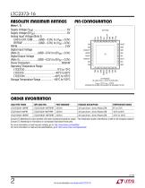
LTC2373-16 Absolute Maximum Ratings UH PACKAGE 32-LEAD (5mm × 5mm) PLASTIC QFN TJMAX = 125°C, θJA = 44°C/W EXPOSED PAD IS GND (PIN 33) MUST BE SOLDERED TO PCB Order Information LEAD FREE FINISH PART MARKING* PACKAGE DESCRIPTION TEMPERATURE RANGE Consult LTC Marketing for parts specified with wider operating temperature ranges. *The temperature grade is identified by a label on the shipping container. Consult LTC Marketing for information on nonstandard lead based finish parts. For more information on lead free part marking, go to: http://www.linear.com/leadfree/ For more information on tape...
Open the catalog to page 2
The l denotes the specifications which apply over the full operating temperature range, otherwise specifications are at TA = 25°C. (Note 4) SYMBOL Absolute Input Range (CH0 to CH7) Absolute Input Range (CH0 to CH7, COM) Fully Differential (Note 5) Pseudo-Differential Unipolar (Note 5) Pseudo-Differential Bipolar (Note 5) Fully Differential Pseudo-Differential Unipolar Pseudo-Differential Bipolar Pseudo-Differential Bipolar and Fully Differential (Note 6) VIN+ – VIN– Input Differential Voltage Range VCM Common Mode Input Range Analog Input Leakage Current Analog Input Capacitance Input...
Open the catalog to page 3
The l denotes the specifications which apply over the full operating temperature range, otherwise specifications are at TA = 25°C. (Note 4) SYMBOL PARAMETER Full-Scale Error Drift Full-Scale Error Match Fully Differential REFBUF = 4.096V (REFBUF Overdriven) (Note 9) Pseudo-Differential Unipolar REFBUF = 4.096V (REFBUF Overdriven) (Note 9) Pseudo-Differential Bipolar REFBUF = 4.096V (REFBUF Overdriven) (Note 9) Fully Differential REFBUF = 4.096V (REFBUF Overdriven) (Note 9) Pseudo-Differential Unipolar REFBUF = 4.096V (REFBUF Overdriven) (Note 9) Pseudo-Differential Bipolar REFBUF = 4.096V...
Open the catalog to page 4
The l denotes the specifications which apply over the full operating temperature range, otherwise specifications are at TA = 25°C and AIN = –1dBFS. (Notes 4, 10) SYMBOL Total Harmonic Distortion Fully Differential fIN = 1kHz, REFIN = 2.048V (REFIN Overdriven) Pseudo-Differential Unipolar fIN = 1kHz, REFIN = 2.048V (REFIN Overdriven) Pseudo-Differential Bipolar fIN = 1kHz, REFIN = 2.048V (REFIN Overdriven) Fully Differential fIN = 1kHz, REFBUF = 5V (REFBUF Overdriven) (Note 9) Pseudo-Differential Unipolar fIN = 1kHz, REFBUF = 5V (REFBUF Overdriven) (Note 9) Pseudo-Differential Bipolar fIN =...
Open the catalog to page 5
LTC2373-16 Reference Buffer Characteristics The l denotes the specifications which apply over the full operating temperature range, otherwise specifications are at TA = 25°C. (Note 4) SYMBOL Reference Buffer Output Voltage REFBUF Input Voltage Range (REFBUF Overdriven) (Notes 5, 9) REFBUF Output Impedance VREFIN = 0V (Buffer Disabled) REFBUF Load Current VREFBUF = 5V (REFBUF Overdriven) (Notes 9, 12) VREFBUF = 5V, Nap Mode (REFBUF Overdriven) (Note 9) Digital Inputs and Digital Outputs The l denotes the specifications which apply over the full operating temperature range, otherwise...
Open the catalog to page 6
The l denotes the specifications which apply over the full operating temperature range, otherwise specifications are at TA = 25°C. (Note 4) tSCK tSCKH tSCKL tSSDISCK SCK Period SCK High Time SCK Low Time SDI Setup Time From SCK↑ SDI Hold Time From SCK↑ SDO Data Valid Delay from SCK↑ SDO Data Remains Valid Delay from SCK↑ CL = 20pF, OVDD = 5.25V CL = 20pF, OVDD = 2.5V CL = 20pF, OVDD = 1.71V CL = 20pF (Note 6) SDO Data Valid Delay from BUSY↓ Bus Enable Time After RDL↓ Bus Relinquish Time After RDL↑ REFBUF Wake-Up Time tWAKE tCNVMRST tMRST1 tVLDMRST tMRST2 CNV↑ to MUX Starts Resetting Delay...
Open the catalog to page 7All ADI catalogs and technical brochures
-
 LTC2068
30 Pages
-
 LTC6373
34 Pages
-
 ADL9006
16 Pages
-
 ADL8104
23 Pages
-
 AD4115
52 Pages
-
 ADUM7702
22 Pages
-
 AD7383
33 Pages
-
 AD7384
33 Pages
-
 AD4114
49 Pages
-
 ADUM7704
22 Pages
-
 AD7134
86 Pages
-
 LTspice IV
53 Pages
-
 New Products Catalog
43 Pages
-
 RF/IF Amplifiers
9 Pages
-
 SAR ADC Drivers
2 Pages
-
 SmartMesh Brochure
8 Pages
-
 INDUSTRIAL SIGNAL CHAIN
24 Pages
-
 AUTOMOTIVE ELECTRONIC SOLUTIONS
48 Pages
-
 Battery Management Solutions
32 Pages
-
 DC/DC uModule Power Products
32 Pages
-
 Wireless & RF Solution
36 Pages
-
 LT6656 - 1
18 Pages


Archived catalogs
-
 New Products Catalog
39 Pages
-
 Power Management for LEDs
24 Pages
-
 High Speed ADC Products Brochure
14 Pages


