
Catalog excerpts

LT3596 3596fa E lectrical Characteristics The l denotes the specifications which apply over the full operating temperature range, otherwise specifications are at TA = 25°C. VIN = 24V, BOOST = 30V, BIAS = 5V, EN/UVLO = 5V, PWM1-3 = 3.3V, CTRL1-3 = CTRLM = TSET = 2V, VOUT = 24V, SYNC = 0V unless otherwise specified. (Note 2) PARAMETER CONDITIONS MIN TYP MAX UNITS VIN Operating Voltage l 6 55 V Quiescent Current from VIN EN/UVLO = 0.4V BIAS = 5V, Not Switching BIAS = 0V, Not Switching 1.3 3 2 4 5 ìA mA mA Minimum BIAS Voltage 3 3.1 V Quiescent Current from BIAS EN/UVLO = 0.4V BIAS = 5V, Not...
Open the catalog to page 3
LT3596 3596fa PARAMETER CONDITIONS MIN TYP MAX UNITS PWM1-3 Input Low Voltage 0.4 V PWM1-3 Input High Voltage 1.6 V PWM1-3 Pin Bias Current 200 nA CTRL1-3 Voltage for Full LED Current 1.2 V CTRL1-3 Pin Bias Current VCTRL1-3 = 6V 200 nA CTRLM Voltage for Full LED Current 1.2 V CTRLM Pin Bias Current VCTRLM = 3V 200 nA FAULT Output Voltage Low IFAULT = 200ìA 0.10 V FAULT Pin Input Leakage Current VFAULT = 25V 200 nA E lectrical Characteristics The l denotes the specifications which apply over the full operating temperature range, otherwise specifications are at TA = 25°C. VIN = 24V, BOOST =...
Open the catalog to page 4
LT3596 3596fa Typical Performance Characteristics UVLO Threshold EN/UVLO Pin Current VREF Voltage Switching Frequency SW and DA Current Limit Switch Voltage Drop VIN Quiescent Current BIAS Quiescent Current VIN, BIAS Shutdown Current TA = 25°C, unless otherwise noted VIN VOLTAGE (V)00VIN CURRENT ( mA)0.40.81.2102030403596 G01501.62.00.20.61.01.41.860T = 125°CT = 25°CT = –40°CVBIAS = 5VBIAS VOLTAGE (V)0BIAS CURRENT ( mA)1.01.52.0203596 G020.50–0.55101525T = 125°CT = 25°CT = –40°CVIN = 24VTEMPERATURE (°C)–500.81.01.4IVIN25753596 G030.60.4–250501001250.201.2CURRENT ( ìA)VIN = 55VVBIAS =...
Open the catalog to page 5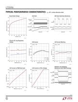
LT3596 3596fa FB and LED Loop Regulation Voltage LED Current LED Current Matching LED Current vs PWM Duty Cycle LED Current vs CTRLn Voltage Adaptive Loop Switching Waveforms (with PWM Dimming) Boost Diode Voltage Soft-Start 60V Buck Switching Waveforms Typical Performance Characteristics TA = 25°C, unless otherwise noted CURRENT (mA)0250BOOST DIODE VOLTAGE ( V)0.41.0501001253596 G100.20.80.675150175EN/UVLO5V/DIVSW50V/DIVVOUT20V/DIV400ìs/DIV3596 G11IL500mA/DIVSW20V/DIVVOUT20V/DIV400ns/DIV3596 G12IL500mA/DIVTEMPERATURE (°C)–50–250.9REGULATION VOLTAGE ( V)1.11.4VFB050753596...
Open the catalog to page 6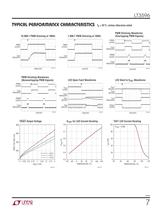
LT3596 3596fa PWM Dimming Waveforms (Nonoverlapping PWM Signals) 10,000:1 PWM Dimming at 100Hz PWM Dimming Waveforms (Overlapping PWM Signals) Typical Performance Characteristics TA = 25°C, unless otherwise noted ILED50mA/DIVPWM2V/DIV200ns/DIV3596 G19 1,000:1 PWM Dimming at 100Hz ILED50mA/DIVPWM2V/DIV2ìs/DIV3596 G20ILED1100mA/DIVILED2100mA/DIVPWM15V/DIVPWM25V/DIV2ms/DIV3596 G21ILED1100mA/DIVILED2100mA/DIVPWM15V/DIVPWM25V/DIV2ms/DIV3596 G22 LED Open-Fault Waveforms ILED1100mA/DIVVSW50V/DIVVLED1V/DIVVOUT20V/DIV20ìs/DIV3596 G23 LED Short to VOUT Waveforms...
Open the catalog to page 7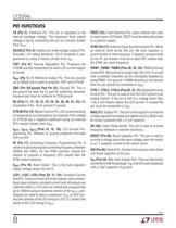
LT3596 3596fa P in Functions FB (Pin 2): Feedback Pin. This pin is regulated to the internal bandgap voltage. The maximum buck output voltage is set by connecting this pin to a resistor divider from VOUT . EN/UVLO (Pin 4): Enable and Undervoltage Lockout Pin. Accurate 1.5V falling threshold. UVLO threshold is programmed by using a resistor divider from VIN. TSET (Pin 6): Thermal Regulation Pin. Programs the LT3596 junction temperature at which LED current begins to derate. VREF (Pin 7): 2V Reference Output Pin. This pin sources up to 200ìA and is used to program TSET and CTRLM. GND (Pin...
Open the catalog to page 8
LT3596 10 3596fa O peration The LT3596 uses a constant-frequency, peak current mode control scheme to provide excellent line and load regulation. Operation is best understood by referring to the Block Diagram (Figure 1). The bias, start-up, reference, oscillator, TSET amplifier and the buck regulator are shared by the three LED current sources. The conversion and control, PWM dimming logic, LED fault detection, and LED drive circuitry are identical for all three current sources. Enable and undervoltage lockout (UVLO) are both controlled by a single pin. If the EN/UVLO pin falls below 1.51V...
Open the catalog to page 10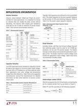
LT3596 11 3596fa A pplications Information Inductor Selection Inductor values between 100ìH and 470ìH are recommended for most applications. It is important to choose an inductor that can handle the peak current without saturating. The inductor DCR (copper wire resistance) must also be low in order to minimize I2R power losses. Table 1 lists several recommended inductors. Table 1. Recommended Inductors PART L (ìH) MAX DCR (Ù) CURRENT RATING (A) VENDOR MSS1038 MSS1038 MSS1246T 100 220 470 0.3 0.76 0.935 1.46 0.99 1.0 Coilcraft www.coilcraft.com CDRH10D68 CDRH12D58R 100 220 470 0.205 0.362...
Open the catalog to page 11
LT3596 12 3596fa A pplications Information In UVLO an internal 5.1ìA (typical) pull-down current source is connected to the pin for programmable UVLO hysteresis. The hysteresis is set according to the following equation: VUVLO(HYST) = 5.1ìA • R2 Care must be taken if too much hysteresis is programmed, the pin voltage might drop too far and cause the current source to saturate. Once the EN/UVLO pin goes below 0.4V, the part enters shutdown. Programming Maximum LED Current Maximum LED current is programmed by placing a resistor (RISETn) between the ISETn pin and ground. RISETn values between...
Open the catalog to page 12
LT3596 13 3596fa A pplications Information Table 6. TSET Programmed Junction Temperature TJ (°C) R1 (kÙ) R2 (kÙ) 85 49.9 97.6 100 49.9 90.9 115 49.9 84.5 The TSET pin must be tied to VREF if the temperature protection feature is not desired. LED1-3CURRENTMAX ILED3596 F05tON(PWM)tPWM Figure 5. LED Current Using PWM Dimming For True Color PWM dimming, the LT3596 provides up to 10,000:1 PWM dimming range at 100Hz. This is done by reducing the duty cycle of the PWMn pin from 100% to 0.01% for a PWM frequency of 100Hz (see Figure 5). This equates to a minimum on time of 1ìs and a maximum period...
Open the catalog to page 13All ADI catalogs and technical brochures
-
 LTC2068
30 Pages
-
 LTC6373
34 Pages
-
 ADL9006
16 Pages
-
 ADL8104
23 Pages
-
 AD4115
52 Pages
-
 ADUM7702
22 Pages
-
 AD7383
33 Pages
-
 AD7384
33 Pages
-
 AD4114
49 Pages
-
 ADUM7704
22 Pages
-
 AD7134
86 Pages
-
 LTspice IV
53 Pages
-
 New Products Catalog
43 Pages
-
 RF/IF Amplifiers
9 Pages
-
 SAR ADC Drivers
2 Pages
-
 SmartMesh Brochure
8 Pages
-
 INDUSTRIAL SIGNAL CHAIN
24 Pages
-
 AUTOMOTIVE ELECTRONIC SOLUTIONS
48 Pages
-
 Battery Management Solutions
32 Pages
-
 DC/DC uModule Power Products
32 Pages
-
 Wireless & RF Solution
36 Pages
-
 LT6656 - 1
18 Pages


Archived catalogs
-
 New Products Catalog
39 Pages
-
 Power Management for LEDs
24 Pages
-
 High Speed ADC Products Brochure
14 Pages


