
Catalog excerpts
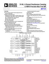
24-Bit, 4-Channel Simultaneous Sampling 1.5 MSPS Precision Alias Free ADC AD7134 Data Sheet FEATURES Sinc3 filter with 50 Hz/60 Hz rejection Crosstalk: 130.7 dBFS Daisy-chaining CRC error checking on data and SPI interface Two power modes: high performance mode and low power mode Power supply: 4.5 V to 5.5 V and 1.65 V to 1.95 V 1.8 V IOVDD level External reference: 4.096 V or 5 V Crystal or external CMOS clock of 48 MHz SPI or pin (standalone) configurable operation Operating temperature range: 0°C to 85°C Available in 8 mm × 8 mm, 56-lead LFCSP with exposed pad Alias free: inherent antialias rejection high performance mode 102.5 dB, typical Excellent ac and dc performance 108 dB dynamic range at ODR = 374 kSPS, FIR filter, typical 137 dB dynamic range at ODR = 10 SPS, sinc3 filter, typical THD: −120 dB typical with 1 kHz input tone Offset error drift: 0.7 µV/°C typical Gain drift: 2 ppm/°C typical INL: ±2 ppm of FSR typical Dynamic range enhancement: 4:1 and 2:1 averaging mode 126 dB, A weighted dynamic range Resistive ADC and reference input Easy to sync: asynchronous sample rate converter Multidevice synchronization with one signal line Programmable data rates from 0.01 kSPS to 1496 kSPS with resolution of 0.01 SPS Option to control output data rate by external signal Linear phase digital filter options Low ripple FIR filter: 32 µdB pass-band ripple, dc to 161.942 kHz Low latency sinc3 filter and sinc6 filter, dc to 391.5 kHz APPLICATIONS Electrical test and measurement Audio test 3-phase power quality analysis Control and hardware in loop verification Sonars Condition monitoring for predictive maintenance Acoustic and material science research and development FUNCTIONAL BLOCK DIAGRAM CLOCK MANAGEMENT CTSD MODULATOR PROGRAMMABLE DIGITAL FILTER ASYNCHRONOUS SAMPLE RATE CONVERTER PROGRAMMABLE DIGITAL FILTER CTSD MODULATOR ASYNCHRONOUS SAMPLE RATE CONVERTER PROGRAMMABLE DIGITAL FILTER CTSD MODULATOR ASYNCHRONOUS SAMPLE RATE CONVERTER CTSD MODULATOR ASYNCHRONOUS SAMPLE RATE CONVERTER PROGRAMMABLE DIGITAL FILTER DIGITAL INTERFACE LOGIC POWER MANAGEMENT Document Feedback Information furnished by Analog Devices is believed to be accurate and reliable. However, no responsibility is assumed by Analog Devices for its use, nor for any infringements of patents or other rights of third parties that may result from its use. Specifications subject to change without notice. No license is granted by implication or otherwise under any patent or patent rights of Analog Devices. Trademarks and registered trademarks are the property of their respective owners. One Technology Way, P.O. Box 9106, Norwood, MA 02062-9106, U.S.A. Tel: 781.329.4700 ©2020 Analog Devices, Inc. All rights reserved. Technical Suppor
Open the catalog to page 1
Data Sheet REVISION HISTORY 4/2020—Revision 0: Initial Version Rev. 0 | Page 2 of 86
Open the catalog to page 2
Data Sheet GENERAL DESCRIPTION no longer requires a high frequency, low jitter master clock from the digital back end to be routed to each ADC. The AD7134 is a quad channel, low noise, simultaneous sampling, precision analog-to-digital converter (ADC) that delivers on functionality, performance, and ease of use. Based on the continuous time sigma-delta (CTSD) modulation scheme, the AD7134 removes the traditionally required switched capacitor circuitry sampling preceding the Σ-Δ modulator, which leads to a relaxation of the ADC input driving requirement. The CTSD architecture also inherently...
Open the catalog to page 3
Data Sheet SPECIFICATIONS AVDD5 = DVDD5 = 4.5 V to 5.5 V, AVDD1V8 = DVDD1V8 = 1.65 V to 1.95 V, CLKVDD = 1.65 V to 1.95 V, LDOIN = 2.6 V to 5.5 V, IOVDD = 1.65 V to 1.95 V, CLKIN = 48 MHz, AGND5 = DGND5 = AGND1V8 = DGND1V8 = IOGND = CLKGND = 0 V, REFIN voltage (Vref) = 4.096 V, high performance mode, input common-mode voltage (Vcm) = 2.048 V, wideband 0.433 Hz x ODR filter, Antialiasing 1 (AA1) mode, unless otherwise noted. Typical values are for Ta = 25°C, AVDD5 = DVDD5 = 5 V, AVDD1V8 = DVDD1V8 = CLKVDD = 1.8 V, LDOIN = 5 V, IOVDD = 1.8 V, unless otherwise noted. Test Conditions/Comments...
Open the catalog to page 4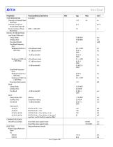
Data Sheet Parameter
Open the catalog to page 6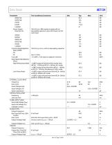
Data Sheet Parameter
Open the catalog to page 7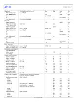
Data Sheet Parameter Test Conditions/Comments Output Voltage Low Input Frequency (fiN) ViNH ViNL Input Capacitance DCLK PIN Output Frequency Output Rise Time/Fall Time (20% to 80%) Output Duty Cycle Output Voltage High Output Voltage Low fIN VINH Vinl Input Capacitance LOGIC INPUTS ViNH Vinl Leakage Currents LOGIC OUTPUTS Output High Voltage (Voh) Output Low Voltage (Vol) 0.2 INTEGRATED LOW DROPOUT (LDO) REGULATOR Output Voltage Input Voltage POWER SUPPLY VOLTAGE AVDD5 to AGND5 DVDD5 to DGND5 AVDD5 to AGND5 DVDD5 to DGND5 DVDD1V8 to DGND AVDD1V8 to AGND1V8 AVDD1V8 to AGND1V8 DVDD1V8 to DGND...
Open the catalog to page 8
Test Conditions/Comments Sinc3 filter, ODR = 1496 kSPS Sinc6 filter, ODR = 1496 kSPS Wideband 0.433 Hz x ODR filter IOVDD CLKVDD _ External LDO mode: AVDD5 = DVDD5 = 5 V, AVDD1V8 = DVDD1V8 = CLKVDD = IOVDD = TOTAL POWER CONSUMPTION High Performance Mode High Performance Mode Full Power-Down Mode Sleep Mode LDOIN = 1.8 V, internal LDO regulator bypassed, XCLKOUT disabled ODR = 374 kSPS, wideband 0.433 Hz x ODR filter 4 channels active 1 channel active 2:1 averaging 4:1 averaging ODR = 2.5 kSPS, 4 channels active ODR = 1496 kSPS, 4 channels active, sinc3 filter ODR = 187 kSPS, wideband 0.433...
Open the catalog to page 9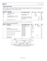
Data Sheet TIMING SPECIFICATIONS AVDD5 = DVDD5 = 4.5 V to 5.5 V, AVDD1V8 = DVDD1V8 = 1.65 V to 1.95 V, CLKVDD = 1.65 V to 1.95 V, IOVDD = 1.65 V to 1.95 V, CLKIN = 48 MHz, AGND5 = DGND5 = AGND1V8 = DGND1V8 = IOGND = CLKGND = 0 V, Ta = 0°C to 85°C, unless otherwise noted. Typical values are at Ta = 25°C, unless otherwise noted. Table 2. Device Clock Timing
Open the catalog to page 10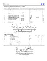
Data Sheet Signal on DOUTx is driven out on the rising edge of DCLK. See Figure 3. Table 4. Data Interface Timing with Free Running DCLK Parameter t9 Description ODR high time DCLK rising edge to ODR rising edge ODR rising edge to DCLK rising edge ODR sampled high to DOUTx active DCLK rising to DOUTx invalid DCLK rising to DOUTx valid Test Conditions/Comments Master mode, tDCLK > tDIGCLK Master mode, tDCLK ≤ tDIGCLK Slave mode, tDCLK > tDIGCLK Slave mode, tDCLK ≤ tDIGCLK Slave mode, tDCLK > tDIGCLK Slave mode, tDCLK ≤ tDIGCLK Slave mode Slave mode Min 2.5 × tDCLK 3 × tDIGCLK 3 × tDCLK 3 ×...
Open the catalog to page 11All ADI catalogs and technical brochures
-
 LTC2068
30 Pages
-
 LTC6373
34 Pages
-
 ADL9006
16 Pages
-
 ADL8104
23 Pages
-
 AD4115
52 Pages
-
 ADUM7702
22 Pages
-
 AD7383
33 Pages
-
 AD7384
33 Pages
-
 AD4114
49 Pages
-
 ADUM7704
22 Pages
-
 LTspice IV
53 Pages
-
 New Products Catalog
43 Pages
-
 RF/IF Amplifiers
9 Pages
-
 SAR ADC Drivers
2 Pages
-
 SmartMesh Brochure
8 Pages
-
 INDUSTRIAL SIGNAL CHAIN
24 Pages
-
 AUTOMOTIVE ELECTRONIC SOLUTIONS
48 Pages
-
 Battery Management Solutions
32 Pages
-
 DC/DC uModule Power Products
32 Pages
-
 Wireless & RF Solution
36 Pages
-
 LT6656 - 1
18 Pages


Archived catalogs
-
 New Products Catalog
39 Pages
-
 Power Management for LEDs
24 Pages
-
 High Speed ADC Products Brochure
14 Pages


