
カタログの抜粋
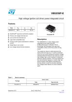
VB525SP-E High voltage ignition coil driver power integrated circuit Features Type Primary coil voltage internally set Coil current limit internally set Logic level compatible input Driving current quasi proportional to collector current Single flag on coil current ECOPACK®: lead free and RoHS compliant Low voltage clamp thermal shutdown Description The VB525SP-E is a high voltage power integrated circuit made using the STMicroelectronics™ VIPower™ M1-3 technology, with Darlington and logic level compatible vertical current flow power driving circuit. The enable pin allows to externally block the switch when the input is on. A built-in protection circuit for coil current limiting and collector voltage clamping allows the device to be used as a smart, high voltage, high current interface in advanced electronic ignition systems. If the input signal from the microcontroller happens to remain high, the device protects itself against overheating by forcing collector current to smoothly decrease (low voltage clamp feature) to avoid undesired spark. Device summary Order codes Package Tube PowerSO-10
カタログの1ページ目を開く
Block diagram and pin description . . . . . . . . . . . . . . . . . . . . . . . . . . . . . 5 Absolute maximum rating . . . . . . . . . . . . . . . . . . . . . . . . . . . . . . . . . . . . . . 7 Thermal data . . . . . . . . . . . . . . . . . . . . . . . . . . . . . . . . . . . . . . . . . . . . . . . 8 Electrical characteristics curves . . . . . . . . . . . . . . . . . . . . . . . . . . . . . . . . 12
カタログの2ページ目を開く
List of tables Table 1. Table 2. Table 3. Table 4. Table 5. Table 6. Table 7. Device summary . . . . . . . . . . . . . . . . . . . . . . . . . . . . . . . . . . . . . . . . . . . . . . . . . . . . . . . . . . 1 Pin function . . . . . . . . . . . . . . . . . . . . . . . . . . . . . . . . . . . . . . . . . . . . . . . . . . . . . . . . . . . . . . 5 Absolute maximum ratings . . . . . . . . . . . . . . . . . . . . . . . . . . . . . . . . . . . . . . . . . . . . . . . . . . 7 Thermal data. . . . . . . . . . . . . . . . . . . . . . . . . . . . . . . . . . . . . . . . . . . . . . . . . . . . . ....
カタログの3ページ目を開く
List of figures Figure 1. Figure 2. Figure 3. Figure 4. Figure 5. Figure 6. Figure 7. Figure 8. Figure 9. Figure 10. Figure 11. Block diagram . . . . . . . . . . . . . . . . . . . . . . . . . . . . . . . . . . . . . . . . . . . . . . . . . . . . . . . . . . . . 5 Connection diagram (top view) . . . . . . . . . . . . . . . . . . . . . . . . . . . . . . . . . . . . . . . . . . . . . . . 6 Switching time for inductive load . . . . . . . . . . . . . . . . . . . . . . . . . . . . . . . . . . . . . . . . . . . . 11 Flag current vs temperature . . . . . . . . . . . . . . . . . . . . . . . . . . ....
カタログの4ページ目を開く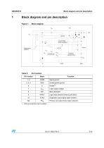
Block diagram and pin description Block diagram and pin description Figure 1. QUASI PROP. BASE CURRENT DIAGNOSTIC OUTPUT THERMAL PROTECTION Signal ground Emitter power ground Logic supply voltage Base darlington Logic input channel (internal pull down) Diagnostic output signal (open emitter) Primary coil output driver (open collector) 1. When grounded the input is enabled
カタログの5ページ目を開く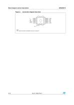
Block diagram and pin description Figure 2. Connection diagram (top view) Note: Pin 1 and pin 5 must be connected to pin2, pin 3 and pin 4
カタログの6ページ目を開く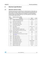
Electrical specifications Electrical specifications Absolute maximum rating Stressing the device above the ratings listed in the “Absolute maximum ratings” tables may cause permanent damage to the device. These are stress ratings only and operation of the device at these or any other conditions above those indicated in the Operating sections of this specification is not implied. Exposure to the conditions in this section for extended periods may affect device reliability. Refer also to the STMicroelectronics SURE Program and other relevant quality documents. Table 3. Absolute maximum...
カタログの7ページ目を開く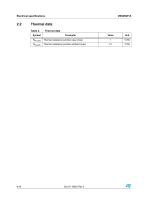
Electrical specifications Thermal data Table 4. Symbol Thermal data Parameter Thermal resistance junction-case (max) Thermal resistance junction-ambient (max)
カタログの8ページ目を開く
Electrical characteristics Electrical characteristics 5.3 V < Vbat < 24 V; VCC = 5 V ±10 %; -40 °C < Tj < 125 °C; Rcoil = 580 mΩ; Lcoil = 3.75 mH unless otherwise specified(a). Table 5. Symbol Electrical characteristics Parameter Test conditions High voltage clamp Power stage saturation voltage Standby supply current Peak DC logic current during on phase Coil current limit Output off-state current High level input voltage Low level input voltage VCC = 5.5 V Input threshold hysteresis High level input current Low level input current VIN = 0.8 V Input active pull down High level flag output...
カタログの9ページ目を開く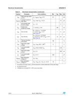
Electrical characteristics Table 5. Electrical characteristics (continued) 1. The primary coil current value lc| must be measured ms after desaturation of the power stage. 3. If ENABLE pin is floating OUT = Off for every input status.
カタログの10ページ目を開く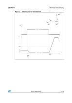
Electrical characteristics Figure 3. Switching time for inductive load Vbat
カタログの11ページ目を開く
Electrical characteristics Electrical characteristics curves Figure 4. Flag current vs temperature Single pulse avalanche energy capability Self clamped inductive switching current vs time Time in Clamp (µsec) Low voltage clamp feature
カタログの12ページ目を開く
Application schematic Application schematic Figure 8. Application diagram Note: ENABLE pin can be alternatively connected to LGND. Principle of operation The VB525SP-E is mainly intended as a high voltage power switch device driven by a logic level input and interfaces directly to a high energy electronic ignition coil. The input VIN of the VB525SP-E is fed from a low power signal generated by an external controller that determines both dwell time and ignition point. During VIN high (≥ 4 V) the VB525SP-E increases current in the coil to the desired, internally set current level. After...
カタログの13ページ目を開く
Application schematic Overvoltage The VB525SP-E can withstand the following transients of the battery line: ● ● -100 V / 2 msec (Ri = 10 Ω) +50 V / 400 msec (Ri = 4.2 Ω, with VIN = 3 V)
カタログの14ページ目を開く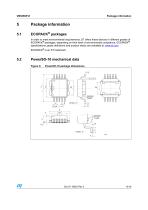
Package information Package information ECOPACK® packages In order to meet environmental requirements, ST offers these devices in different grades of ECOPACK® packages, depending on their level of environmental compliance. ECOPACK® specifications, grade definitions and product status are available at: www.st.com. ECOPACK® is an ST trademark. PowerSO-10 mechanical data Figure 9. SEATING PLANE
カタログの15ページ目を開くSTMicroelectronicsのすべてのカタログと技術パンフレット
-
 STGW30NC60KD
14 ページ
-
 STGB14NC60K STGD14NC60K
16 ページ
-
 HD1750FX
8 ページ
-
 TDA75610SLV
42 ページ
-
 TDA7391
13 ページ
-
 TDA7376B
15 ページ
-
 TDA7375V
15 ページ
-
 TDA2005
25 ページ
-
 L4989D, L4989MD
19 ページ
-
 L4938ED L4938EPD
20 ページ
-
 L4949ED-E L4949EP-E
19 ページ
-
 L4925
L492514 ページ
-
 FDA903U
80 ページ
-
 FDA803U
76 ページ
-
 FDA903D
82 ページ
-
 FDA803D
78 ページ
-
 BALF-SPI2-02D3
13 ページ
-
 LIS2DTW12
65 ページ
-
 VL53L0X
40 ページ
-
 LPS22HH
59 ページ
-
 M40SZ100W
20 ページ
-
 A1C15S12M3
17 ページ
-
 TSX923
32 ページ
-
 TS1851
24 ページ
-
 LMV321
17 ページ
-
 TDA2003LG
8 ページ
-
 TSA1204 DUAL CHANNEL
31 ページ


カタログアーカイブ
-
 NEATSwitch
6 ページ


