
カタログの抜粋
TDA7303 Digital controlled stereo audio processor with loudness Features ■ Input multiplexer: – 3 stereo inputs – Selectable input gain for optimal adaptation to different sources Volume control in 1.25 dB steps Loudness function Treble and bass controL Four speaker attenuators: – 4 independent speakers control in 1.25d B steps for balance and fader facilities – Independent mute function All functions programmable via serial I2C bus Description The TDA7303 is a volume, tone (bass and treble) balance (left/right) and fader (front/rear) processor for quality audio applications in car radio, Hi-Fi and portable systems. Table 1. Selectable input gain and external loudness function are provided. Control is accomplished by serial I2C bus microprocessor interface. The AC signal setting is obtained by resistor networks and switches combined with operational amplifiers. Thanks to the used bipolar/CMOS technology, low distortion, low noise and low DC stepping are obtained. Device summary Order code
カタログの1ページ目を開く
Block, test and pin diagrams . . . . . . . . . . . . . . . . . . . . . . . . . . . . . . . . . . 5 1.1 1.2 Quick reference data . . . . . . . . . . . . . . . . . . . . . . . . . . . . . . . . . . . . . . . . . 7 Absolute maximum ratings . . . . . . . . . . . . . . . . . . . . . . . . . . . . . . . . . . . . . 7 Electrical characteristics curves . . . . . . . . . . . . . . . . . . . . . . . . . . . . . . . . 10 Start and stop conditions . . . . . . . . . . . . . . . . . . . . . . . . . . . . . . . . . . . . . 13 Transmission without acknowledge . . . . . . . . . . . . . . . . . . . . . . . ....
カタログの2ページ目を開く
List of tables Table 1. Table 2. Table 3. Table 4. Table 5. Table 6. Table 7. Table 8. Table 9. Table 10. Table 11. Table 12. Device summary . . . . . . . . . . . . . . . . . . . . . . . . . . . . . . . . . . . . . . . . . . . . . . . . . . . . . . . . . . 1 Absolute maximum ratings . . . . . . . . . . . . . . . . . . . . . . . . . . . . . . . . . . . . . . . . . . . . . . . . . . 7 Quick reference data . . . . . . . . . . . . . . . . . . . . . . . . . . . . . . . . . . . . . . . . . . . . . . . . . . . . . . 7 Thermal data. . . . . . . . . . . . . . . . . . . . . . . . . . . . . . . . . ....
カタログの3ページ目を開く
List of figures Figure 1. Figure 2. Figure 3. Figure 4. Figure 5. Figure 6. Figure 7. Figure 8. Figure 9. Figure 10. Figure 11. Figure 12. Figure 13. Figure 14. Figure 15. Figure 16. Figure 17. Figure 18. Figure 19. Figure 20. Figure 21. Figure 22. Figure 23. Figure 24. Block diagram . . . . . . . . . . . . . . . . . . . . . . . . . . . . . . . . . . . . . . . . . . . . . . . . . . . . . . . . . . . . 5 Test circuit . . . . . . . . . . . . . . . . . . . . . . . . . . . . . . . . . . . . . . . . . . . . . . . . . . . . . . . . . . . . . . 6 Pin connection (top view) . . . . . . . . . . . . ....
カタログの4ページ目を開く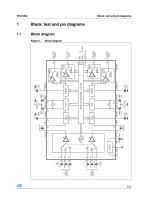
INPUT SELECTOR + GAIN SERIAL BUS DECODER + LATCHES Block, test and pin diagrams RIGHT INPUTS LEFT INPUTS TDA7303 Block, test and pin diagrams Block diagram Block diagram
カタログの5ページ目を開く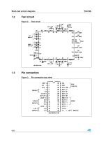
Block, test and pin diagrams Test circuit Figure 2. Test circuit (LiliHa>l TBOUTCD^INID S22uF |_HI_| g lBBnF g lBBnF Figure 3. Pin connection (top view) LEFT INPUTS
カタログの6ページ目を開く
Electrical specifications Electrical specifications Absolute maximum ratings Table 2. Absolute maximum ratings Operating supply voltage Ambient temperature Storage temperature range Quick reference data Table 3. Quick reference data Supply voltage Max. input signal handling Total harmonic distortion V = 1 Vrms; f = 1 kHz Signal to noise ratio Volume control 1.25d B step Bass and treble control 2 dB step Fader and balance control 1.25 dB step Input gain 3.75 dB step1.25 dB step Mute attenuation Thermal data Table 4. Symbol Rth j-pins Thermal data Parameter Thermal resistance junction to pins
カタログの7ページ目を開く
Electrical specifications Electrical characteristics Electrical characteristics (Tamb = 25 °C, VS = 9 V, RL = 10 k, RG = 600 , all control flat (G = 0), f = 1 kHz unless otherwise specified) Test condition Supply voltage Supply current Ripple rejection Input resistance Clipping level Input separation Output load resistance Step resolution Input noise Input resistance CRANGE Control range Step resolution Tracking error Speaker attenuators Crange Control range Step resolution Attenuation set error Output mute attenuation Control range Step resolution
カタログの8ページ目を開く
Electrical specifications Electrical characteristics (continued) (Tamb = 25 °C, VS = 9 V, RL = 10 k, RG = 600 , all control flat (G = 0), f = 1 kHz unless otherwise specified) Test condition Internal feedback resistance Treble control (1) Gt TSTEP Control range Step Resolution Audio outputs VOCL Clipping level Output load resistance Output load capacitance Output resistance General BW = 20-20 kHz, flat output muted all gains = 0 dB Signal to noise ratio Channel separation left/right Total tracking error Input high voltage Input current Output voltage SDA acknowledge 1. Bass and treble...
カタログの9ページ目を開く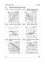
Electrical specifications 2.5 Electrical characteristics curves Figure 4. Loudness vs. volume attenuation Figure 5. Loudness vs. frequency (CLOUD =
カタログの10ページ目を開く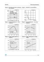
Electrical specifications Figure 10. Distortion and noise vs. frequency Figure 11. Distortion vs. load resistance
カタログの11ページ目を開く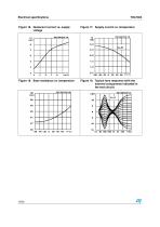
Electrical specifications Figure 16. Quiescent current vs. supply Figure 17. Supply current vs. temperature Figure 18. Bass resistance vs. temperature Figure 19. Typical tone response (with the external components indicated in
カタログの12ページ目を開く
I2C bus interface Data transmission from microprocessor to the TDA7303 and viceversa takes place through the 2 wires I2C bus interface, consisting of the two lines SDA and SCL (pull-up resistors to positive supply voltage must be connected). Data validity As shown in Figure 20, the data on the SDA line must be stable during the high period of the clock. The high and low state of the data line can only change when the clock signal on the SCL line is lOW. Start and stop conditions As shown in Figure 21 a start condition is a high to low transition of the SDA line while SCL is high. The stop...
カタログの13ページ目を開くSTMicroelectronicsのすべてのカタログと技術パンフレット
-
 STGW30NC60KD
14 ページ
-
 STGB14NC60K STGD14NC60K
16 ページ
-
 HD1750FX
8 ページ
-
 TDA75610SLV
42 ページ
-
 TDA7391
13 ページ
-
 TDA7376B
15 ページ
-
 TDA7375V
15 ページ
-
 TDA2005
25 ページ
-
 L4989D, L4989MD
19 ページ
-
 L4938ED L4938EPD
20 ページ
-
 L4949ED-E L4949EP-E
19 ページ
-
 L4925
L492514 ページ
-
 FDA903U
80 ページ
-
 FDA803U
76 ページ
-
 FDA903D
82 ページ
-
 FDA803D
78 ページ
-
 BALF-SPI2-02D3
13 ページ
-
 LIS2DTW12
65 ページ
-
 VL53L0X
40 ページ
-
 LPS22HH
59 ページ
-
 M40SZ100W
20 ページ
-
 A1C15S12M3
17 ページ
-
 TSX923
32 ページ
-
 TS1851
24 ページ
-
 LMV321
17 ページ
-
 TDA2003LG
8 ページ
-
 TSA1204 DUAL CHANNEL
31 ページ


カタログアーカイブ
-
 NEATSwitch
6 ページ


