ST485EC +/-15 kV ESD protected, low power RS-485/RS-422 transceiver Active Save to myST send to a friend
1 /
18ページ

カタログの抜粋
February 2009 Rev 14 1/18 18 ST485EB ST485EC - ST485EX ±15 kV ESD protected, low power RS-485/RS-422 transceiver Features ¡ Low quiescent current: 300 ìA ¡ Designed for RS-485 interface application ¡ - 7 V to 12 V common mode input voltage range ¡ Driver maintains high impedance in 3-state or with the power OFF ¡ 70 mV typical input hysteresis ¡ 30 ns propagation delay, 5 ns skew ¡ Operates from a single 5 V supply ¡ Current limiting and thermal shutdown for driver overload protection ¡ ESD protection: – ± 15 kV (HBM) – ± 8 kV (IEC-1000-4-2 contact discharge) ¡ Allows up to 256 transceivers on the bus Description The ST485E is a low power transceiver for RS- 485 and RS-422 communication. Each driver output and receiver input is protected against ± 15 kV electrostatic discharge (HBM) (ESD) shocks, without latch-up. These parts contain one driver and one receiver in half duplex configuration. This transceiver draws 300 ìA (typ.) of supply current when unloaded or fully loaded with disabled drivers. It operates from a single 5 V supply. Driver is short-circuit current limited and is protected against excessive power dissipation by thermal shutdown circuitry that place the driver outputs into a high-impedance state. The ST485E is designed for bi-directional data communications on multipoint bus transmission lines (half-duplex applications). SO-8 Table 1. Device summary Order codes Temperature range Package Packaging ST485EBD - 40 to 85 °C SO-8 (tube) 100 parts per tube / 20 tube per box ST485ECDR 0 to 70 °C SO-8 (tape and reel) 2500 parts per reel ST485EBDR - 40 to 85 °C SO-8 (tape and reel) 2500 parts per reel ST485EXDR - 55 to 125 °C SO-8 (tape and reel) 2500 parts per reel www.st.com
カタログの1ページ目を開く
Contents ST485EB - ST485EC - ST485EX 2/18 Contents 1 Pin configuration . . . . . . . . . . . . . . . . . . . . . . . . . . . . . . . . . . . . . . . . . . . 3 2 Truth tables . . . . . . . . . . . . . . . . . . . . . . . . . . . . . . . . . . . . . . . . . . . . . . . . 4 3 Maximum ratings . . . . . . . . . . . . . . . . . . . . . . . . . . . . . . . . . . . . . . . . . . . 5 4 Electrical characteristics . . . . . . . . . . . . . . . . . . . . . . . . . . . . . . . . . . . . . 6 5 Test circuit and typical characteristics . . . . . . . . . . . . . . . . . . . . . . . . . . 9 6 Package...
カタログの2ページ目を開く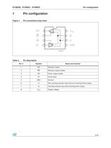
ST485EB - ST485EC - ST485EX Pin configuration 3/18 1 Pin configuration Figure 1. Pin connections (top view) Table 2. Pin description Pin n° Symbol Name and function 1 RO Receiver output 2 RE Receiver output enable 3 DE Driver output enable 4 DI Driver input 5 GND Ground 6 A Non-inverting receiver input and non-inverting driver output 7 B Inverting receiver input and inverting driver output 8 VCC Supply voltage
カタログの3ページ目を開く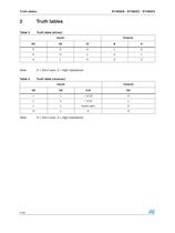
Truth tables ST485EB - ST485EC - ST485EX 4/18 2 Truth tables Note: X = Don’t care; Z = High impedance Note: X = Don’t care; Z = High impedance Table 3. Truth table (driver) Inputs Outputs RE DE DI B A X H H L H X H L H L X L X Z Z Table 4. Truth table (receiver) Inputs Outputs RE DE A-B RO L L +0.2V H L L -0.2V L L L Inputs open H H L X Z
カタログの4ページ目を開く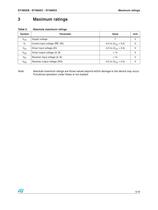
ST485EB - ST485EC - ST485EX Maximum ratings 5/18 3 Maximum ratings Note: Absolute maximum ratings are those values beyond which damage to the device may occur. Functional operation under these is not implied. Table 5. Absolute maximum ratings Symbol Parameter Value Unit VCC Supply voltage 7 V VI Control input voltage (RE, DE) -0.5 to (VCC + 0.5) V VDI Driver input voltage (DI) -0.5 to (VCC + 0.5) V VDO Driver output voltage (A, B) ± 14 V VRI Receiver input voltage (A, B) ± 14 V VRO Receiver output voltage (RO) -0.5 to (VCC + 0.5) V
カタログの5ページ目を開く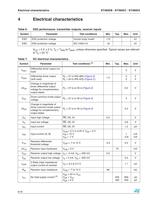
Electrical characteristics ST485EB - ST485EC - ST485EX 6/18 4 Electrical characteristics VCC = 5 V ± 5 %, TA = TMIN to TMAX, unless otherwise specified. Typical values are referred to TA = 25 °C Table 6. ESD performance: transmitter outputs, receiver inputs Symbol Parameter Test conditions Min. Typ. Max. Unit ESD ESD protection voltage Human body model ±15 kV ESD ESD protection voltage IEC-1000-4-2 ±8 kV Table 7. DC electrical characteristics Symbol Parameter Test conditions (1) Min. Typ. Max. Unit VOD1 Differential driver output (no load) 5 V VOD2 Differential driver output (with load) RL...
カタログの6ページ目を開く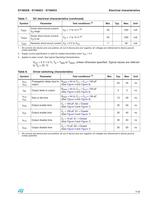
ST485EB - ST485EC - ST485EX Electrical characteristics 7/18 VCC = 5 V ± 5 %, TA = TMIN to TMAX, unless otherwise specified. Typical values are referred to TA = 25 °C IOSD1 Driver short-circuit current, VO=High VO = -7 to 12 V (3) 35 250 mA IOSD2 Driver short-circuit current, VO=Low VO = -7 to 12 V (3) 35 250 mA IOSR Receiver short-circuit current VO = 0 V to VCC 7 95 mA 1. All currents into device pins are positive; all out of device pins are negative; all voltages are referenced to device ground unless specified. 2. Supply current specification is valid for loaded transmitters when VDE = 0...
カタログの7ページ目を開く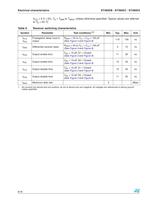
Electrical characteristics ST485EB - ST485EC - ST485EX 8/18 VCC = 5 V ± 5%, TA = TMIN to TMAX, unless otherwise specified. Typical values are referred to TA = 25 °C Table 9. Receiver switching characteristics Symbol Parameter Test conditions (1) Min. Typ. Max. Unit tPLH tPHL Propagation delay input to output RDIFF = 54 Ù, CL1 = CL2 = 100 pF (See Figure 4 and Figure 8) 110 130 ns tSKD Differential receiver skew RDIFF = 54 Ù, CL1 = CL2 = 100 pF (See Figure 4 and Figure 8) 5 10 ns tPZH Output enable time CRL = 15 pF, S1 = Closed (See Figure 2 and Figure 9) 11 35 ns tPZL Output enable time CRL...
カタログの8ページ目を開く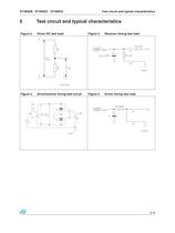
ST485EB - ST485EC - ST485EX Test circuit and typical characteristics 9/18 5 Test circuit and typical characteristics Figure 2. Driver DC test load Figure 3. Receiver timing test load Figure 4. Drive/receiver timing test circuit Figure 5. Driver timing test load
カタログの9ページ目を開く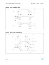
Test circuit and typical characteristics ST485EB - ST485EC - ST485EX 10/18 Figure 6. Driver propagation delay Figure 7. Driver enable and disable time
カタログの10ページ目を開くSTMicroelectronicsのすべてのカタログと技術パンフレット
-
 STGW30NC60KD
14 ページ
-
 STGB14NC60K STGD14NC60K
16 ページ
-
 HD1750FX
8 ページ
-
 TDA75610SLV
42 ページ
-
 TDA7391
13 ページ
-
 TDA7376B
15 ページ
-
 TDA7375V
15 ページ
-
 TDA2005
25 ページ
-
 L4989D, L4989MD
19 ページ
-
 L4938ED L4938EPD
20 ページ
-
 L4949ED-E L4949EP-E
19 ページ
-
 L4925
L492514 ページ
-
 FDA903U
80 ページ
-
 FDA803U
76 ページ
-
 FDA903D
82 ページ
-
 FDA803D
78 ページ
-
 BALF-SPI2-02D3
13 ページ
-
 LIS2DTW12
65 ページ
-
 VL53L0X
40 ページ
-
 LPS22HH
59 ページ
-
 M40SZ100W
20 ページ
-
 A1C15S12M3
17 ページ
-
 TSX923
32 ページ
-
 TS1851
24 ページ
-
 LMV321
17 ページ
-
 TDA2003LG
8 ページ
-
 TSA1204 DUAL CHANNEL
31 ページ


カタログアーカイブ
-
 NEATSwitch
6 ページ


